Michael A. Scarpulla

20 papers on arXiv

Academic Profile

Name: M. Scarpulla
Total Papers: 3

Statistics

arXiv Papers 20
Total Publications 3

Papers on arXiv

Thumbnail for Epitaxial Growth of Rutile GeO$_2$ via MOCVD

Epitaxial Growth of Rutile GeO$_2$ via MOCVD

Rutile Germanium Dioxide (r-GeO$_2$) has been identified as an ultrawide bandgap (UWBG) semiconductor recently, featuring a bandgap of 4.68 eV, comparable to Ga$_2$O$_3$ but offering bipolar dopabil...

Thumbnail for Growth of GeO2 on R-plane and C-plane Sapphires by MOCVD

Growth of GeO2 on R-plane and C-plane Sapphires by MOCVD

Rutile Germanium Dioxide (GeO2) has been recently theoretically identified as an ultrawide bandgap (UWBG) semiconductor with bandgap 4.68 eV similar to Ga2O3 but having bipolar dopability and ~2x hi...

Thumbnail for Quantification of the strong, phonon-induced Urbach tails in
  \b{eta}-Ga2O3 and their implications on electrical breakdown

Quantification of the strong, phonon-induced Urbach tails in \b{eta}-Ga2O3 and their implications on electrical breakdown

In ultrawide bandgap (UWBG) nitride and oxide semiconductors, increased bandgap (Eg) correlates with greater ionicity and strong electron-phonon coupling. This limits mobility through polar optical ...

Thumbnail for Utilizing (Al, Ga)2O3/Ga2O3 superlattices to measure cation vacancy
  diffusion and vacancy-concentration-dependent diffusion of Al, Sn, and Fe in
  \b{eta} -Ga2O3

Utilizing (Al, Ga)2O3/Ga2O3 superlattices to measure cation vacancy diffusion and vacancy-concentration-dependent diffusion of Al, Sn, and Fe in \b{eta} -Ga2O3

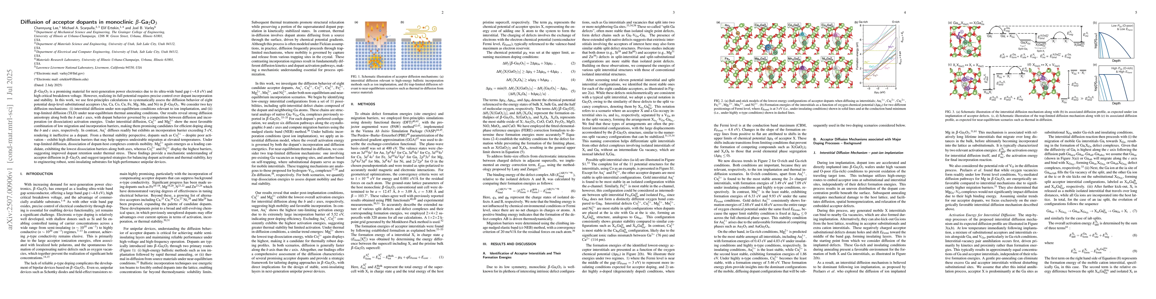
Diffusion of native defects such as vacancies and their interactions with impurities are fundamental in semiconductor crystal growth, device processing, and long-term aging of equilibration and tran...

Thumbnail for Investigation of Ga interstitial and vacancy diffusion in
  $\beta$-Ga$_2$O$_3$ via split defects: a direct approach via master diffusion
  equations

Investigation of Ga interstitial and vacancy diffusion in $\beta$-Ga$_2$O$_3$ via split defects: a direct approach via master diffusion equations

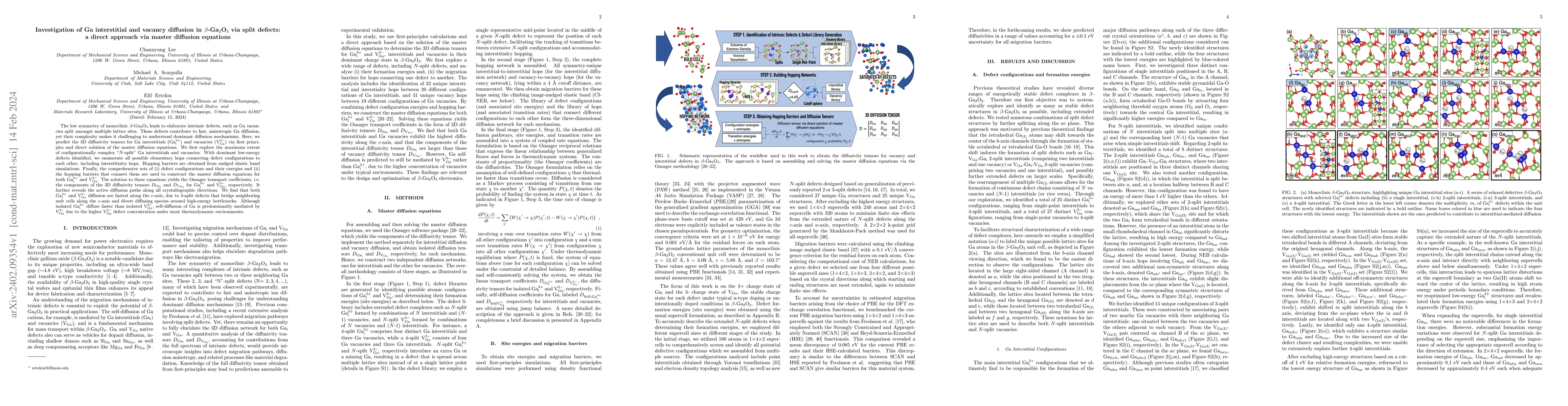
The low symmetry of monoclinic $\beta$-Ga$_2$O$_3$ leads to elaborate intrinsic defects, such as Ga vacancies split amongst multiple lattice sites. These defects contribute to fast, anisotropic Ga d...

Thumbnail for Efficiency versus effort: a better way to compare best photovoltaic
  research cell efficiencies?

Efficiency versus effort: a better way to compare best photovoltaic research cell efficiencies?

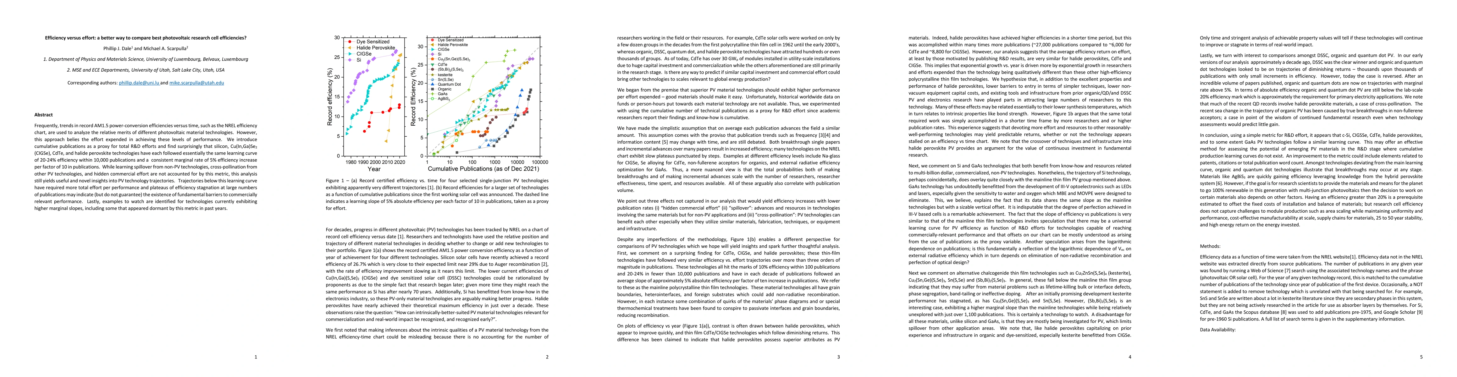
Frequently, trends in record AM1.5 power-conversion efficiencies versus time, such as the NREL efficiency chart, are used to analyze the relative merits of different photovoltaic material technologi...

Thumbnail for In-situ dielectric Al2O3/\b{eta}-Ga2O3 Interfaces Grown Using
  Metal-organic Chemical Vapor Deposition

In-situ dielectric Al2O3/\b{eta}-Ga2O3 Interfaces Grown Using Metal-organic Chemical Vapor Deposition

High-quality dielectric-semiconductor interfaces are critical for reliable high-performance transistors. We report the in-situ metalorganic chemical vapor deposition (MOCVD) of Al$_2$O$_3$ on $\beta...

Thumbnail for N-type doping of LPCVD-grown \b{eta}-Ga2O3 thin films using solid-source
  germanium

N-type doping of LPCVD-grown \b{eta}-Ga2O3 thin films using solid-source germanium

We report on the growth and characterization of Ge-doped \b{eta}-Ga2O3 thin films using a solid germanium source. \b{eta}-Ga2O3 thin films were grown using a low-pressure chemical vapor deposition (...

Thumbnail for Defect states and their electric field-enhanced electron thermal
  emission in heavily Zr-doped beta-Ga2O3 crystals

Defect states and their electric field-enhanced electron thermal emission in heavily Zr-doped beta-Ga2O3 crystals

Performing deep level transient spectroscopy (DLTS) on Schottky diodes, we investigated defect levels below the conduction band minima (Ec) in Czochralski (CZ) grown unintentionally-doped (UID) and ...

Thumbnail for The anisotropic quasi-static permittivity of single-crystal beta-Ga2O3

The anisotropic quasi-static permittivity of single-crystal beta-Ga2O3

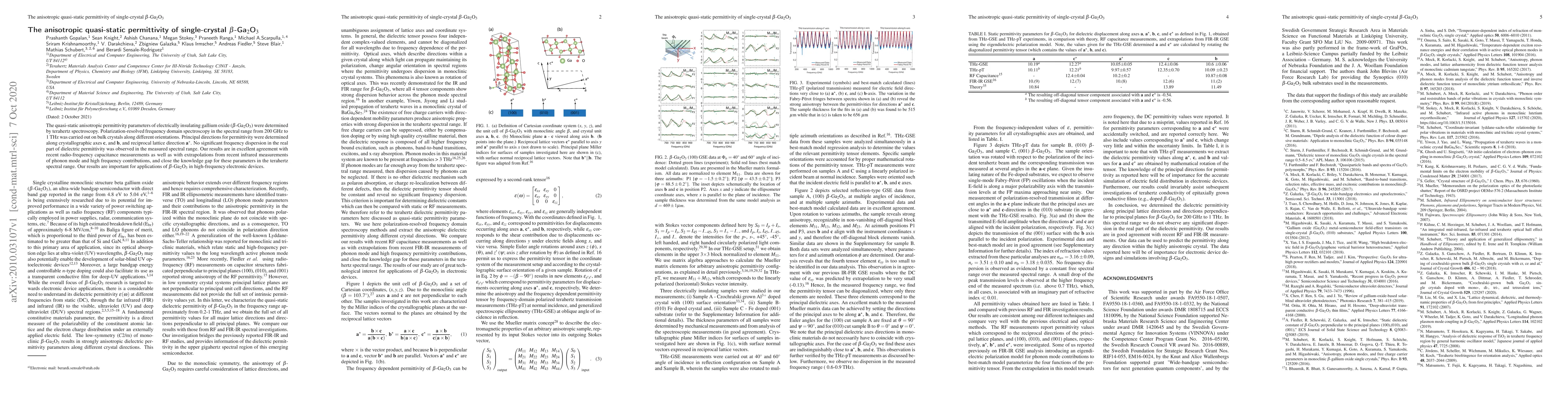
The quasi-static anisotropic permittivity parameters of electrically insulating gallium oxide (beta-Ga2O3) were determined by terahertz spectroscopy. Polarization-resolved frequency domain spectrosc...

Thumbnail for Oxygen annealing induced changes in defects within beta-Ga2O3 epitaxial
  films measured using photoluminescence

Oxygen annealing induced changes in defects within beta-Ga2O3 epitaxial films measured using photoluminescence

In this work, we use photoluminescence spectroscopy (PL) to monitor changes in the UV, UV', blue, and green emission bands from n-type (010) Ga2O3 films grown by metalorganic vapor phase epitaxy (MO...

Thumbnail for On the origin of red luminescence from iron-doped beta-Ga2O3 bulk
  crystals

On the origin of red luminescence from iron-doped beta-Ga2O3 bulk crystals

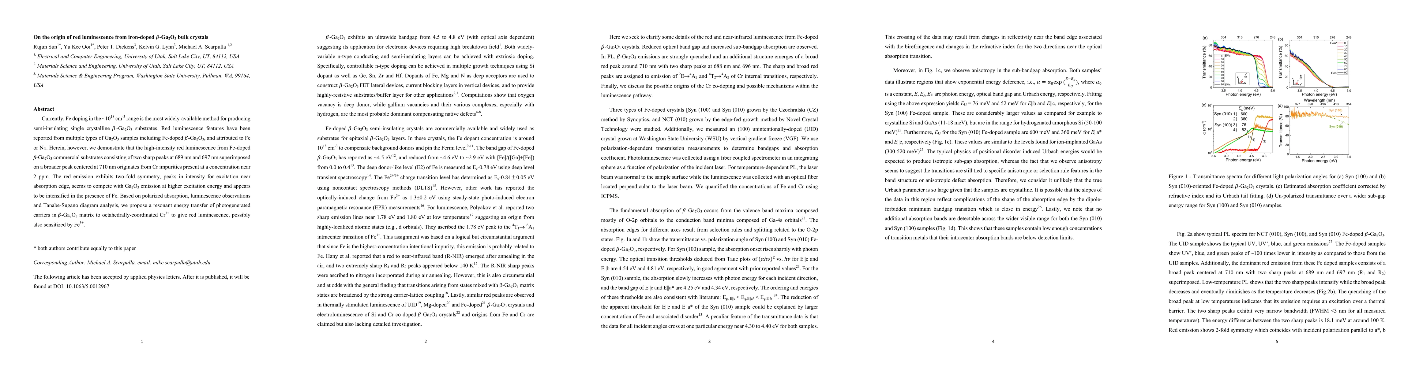
Currently, Fe doping in the ~10^18 cm-3 range is the most widely-available method for producing semi-insulating single crystalline beta-Ga2O3 substrates. Red luminescence features have been reported...

Thumbnail for Schottky Barrier Height Engineering In $\beta$-Ga$_2$O$_3$ Using SiO$_2$
  Interlayer Dielectric

Schottky Barrier Height Engineering In $\beta$-Ga$_2$O$_3$ Using SiO$_2$ Interlayer Dielectric

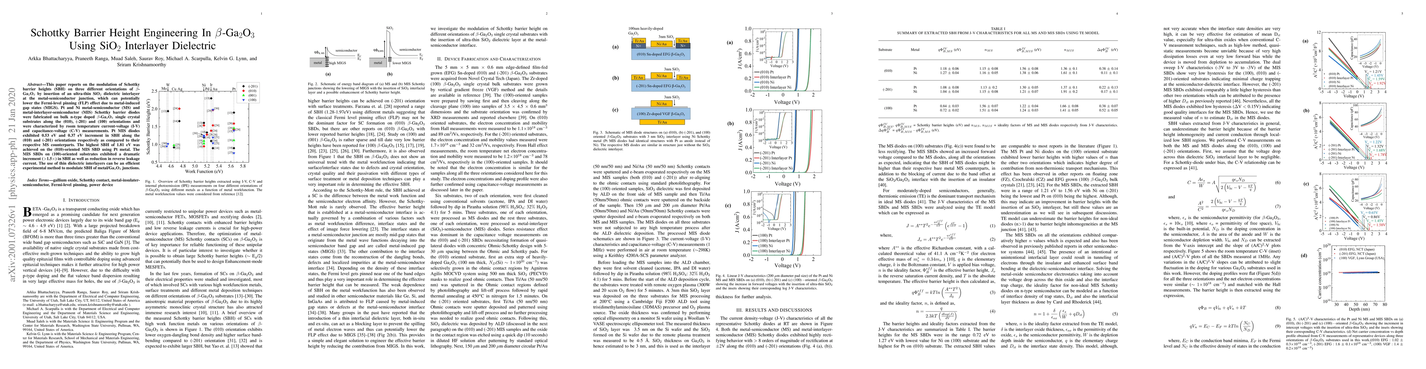
This paper reports on the modulation of Schottky barrier heights (SBH) on three different orientations of $\beta$-Ga$_2$O$_3$ by insertion of an ultra-thin SiO$_2$ dielectric interlayer at the metal...

Thumbnail for Quantitative Modeling of Point Defects in $β$-Ga2O3 Combining Hybrid
  Functional Energetics with Semiconductor and Processes Thermodynamics

Quantitative Modeling of Point Defects in $β$-Ga2O3 Combining Hybrid Functional Energetics with Semiconductor and Processes Thermodynamics

B-gallium oxide (B-Ga2O3) is of high interest for power electronics because of its unique combination of melt growth, epitaxial growth, n-type dopability, ultrawide bandgap, and high critical field. O...

Thumbnail for Degradation of 2.4-kV $Ga_{2}O_{3}$ Schottky Barrier Diode at High
  Temperatures up to 500 °C

Degradation of 2.4-kV $Ga_{2}O_{3}$ Schottky Barrier Diode at High Temperatures up to 500 °C

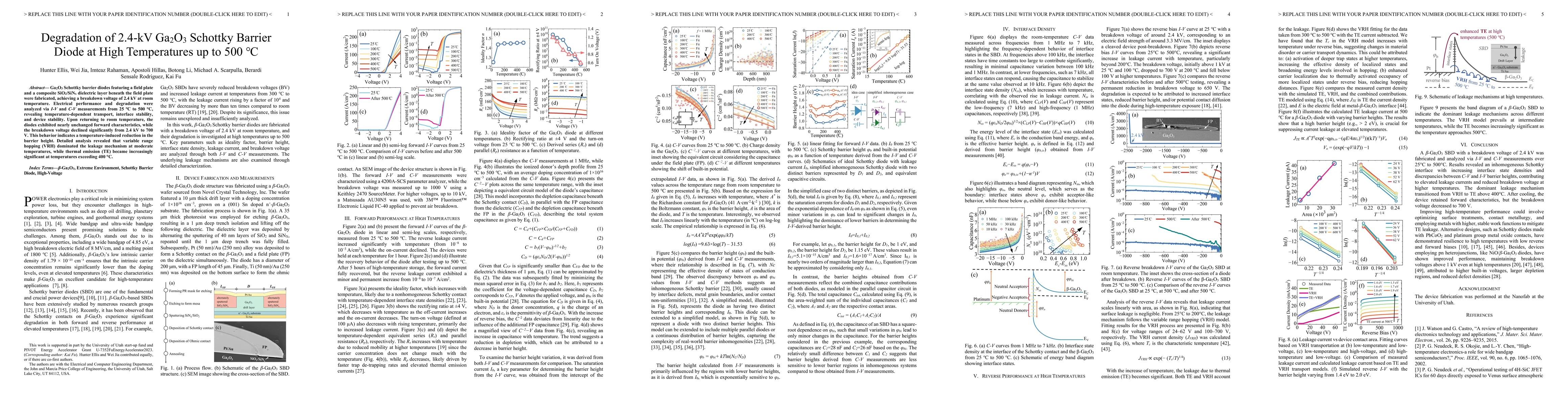
Ga2O3 Schottky barrier diodes featuring a field plate and a composite SiO2/SiNx dielectric layer beneath the field plate were fabricated, achieving a breakdown voltage of 2.4 kV at room temperature. E...

Thumbnail for Diffusion of acceptor dopants in monoclinic $β$-Ga$_2$O$_3$

Diffusion of acceptor dopants in monoclinic $β$-Ga$_2$O$_3$

$\beta$-Ga$_2$O$_3$ is a leading ultra-wide band gap semiconductor, but its performance depends on precise control over dopant incorporation and stability. In this work, we use first-principles calcul...

Thumbnail for Phase Competition and Rutile Phase Stabilization of Growing GeO2 Films
  by MOCVD

Phase Competition and Rutile Phase Stabilization of Growing GeO2 Films by MOCVD

Rutile germanium dioxide (r-GeO2) is an ultra-wide bandgap semiconductor with potential for ambipolar doping, making it a promising candidate for next-generation power electronics and optoelectronics....

Thumbnail for High thermal conductivity of rutile-GeO$_2$ films grown by MOCVD:
  $52.9~\mathrm{W\,m^{-1}\,K^{-1}}$

High thermal conductivity of rutile-GeO$_2$ films grown by MOCVD: $52.9~\mathrm{W\,m^{-1}\,K^{-1}}$

Rutile germanium dioxide (r-GeO2) has recently emerged as a promising ultrawide-bandgap (UWBG) semiconductor owing to its wide bandgap (~4.4-5.1 eV), ambipolar doping potential, and high theoretical t...

Thumbnail for In situ Study of p-NiO Film Quality at High Temperatures up to 1100 deg C

In situ Study of p-NiO Film Quality at High Temperatures up to 1100 deg C

NiO is a promising p-type material for photovoltaics and power electronics, but its temperature limits remain unclear. Using in situ high-temperature X-ray diffraction (HT-XRD) from 30 to 1100 C, we t...

Thumbnail for Impacts of Fermi Level Pinning at Hole-Selective Contacts in CdSeTe/CdTe Solar Cells

Impacts of Fermi Level Pinning at Hole-Selective Contacts in CdSeTe/CdTe Solar Cells

P-type doped CdTe free surfaces Schottky contacts, and even interfaces with isostructural p-ZnTe frequently exhibit downward band bending and moderate to high recombination velocities. Fermi level pin...

This website uses cookies to ensure you get the best experience. Learn more