Academic Profile
Statistics
Similar Authors
Papers on arXiv
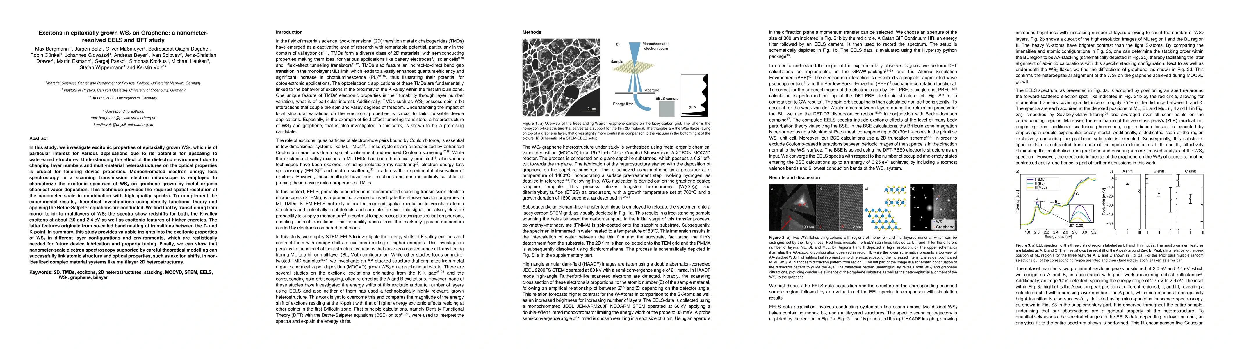
In this study, we investigate excitonic properties of epitaxially grown WS2, which is of particular interest for various applications due to its potential for upscaling to wafer sized structures. Un...
Two-dimensional (2D) materials have received a lot of interest over the past decade. Especially van der Waals (vdW) 2D materials, such as transition metal dichalcogenides (TMDCs), and their heterost...
Two-dimensional (2D) materials are considered for numerous applications in microelectronics, although several challenges remain when integrating them into functional devices. Weak adhesion is one of...
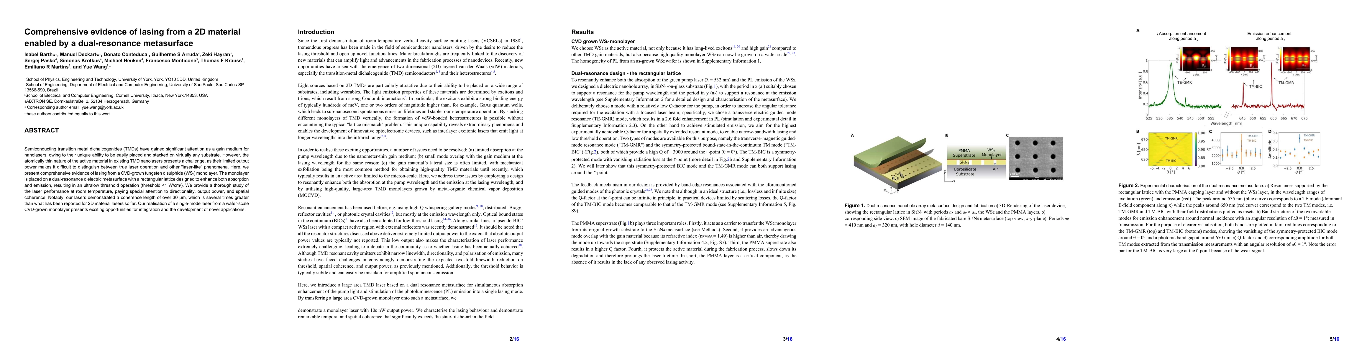
Semiconducting transition metal dichalcogenides (TMDs) have gained significant attention as a gain medium for nanolasers, owing to their unique ability to be easily placed and stacked on virtually a...
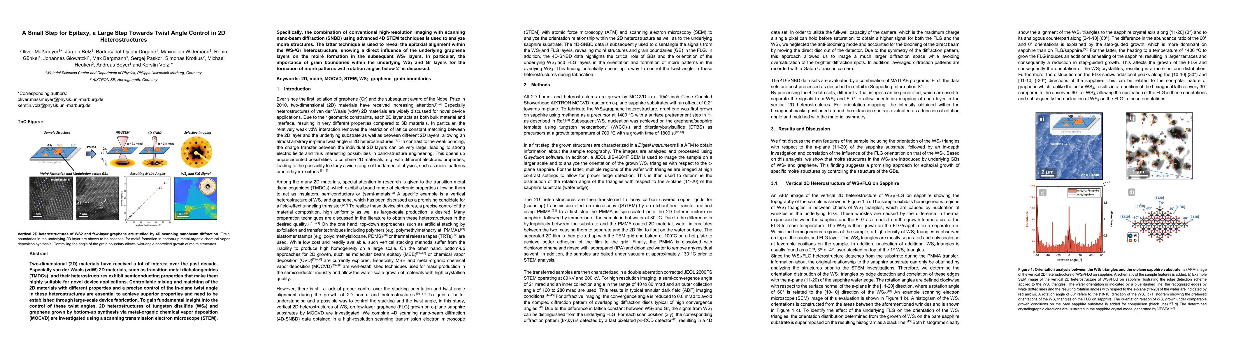
Heterostacks formed by combining two-dimensional materials show novel properties which are of great interest for new applications in electronics, photonics and even twistronics, the new emerging fie...
Epitaxial growth has become a promising route to achieve highly crystalline continuous two-dimensional layers. However, high-quality layer production with expected electrical properties is still cha...
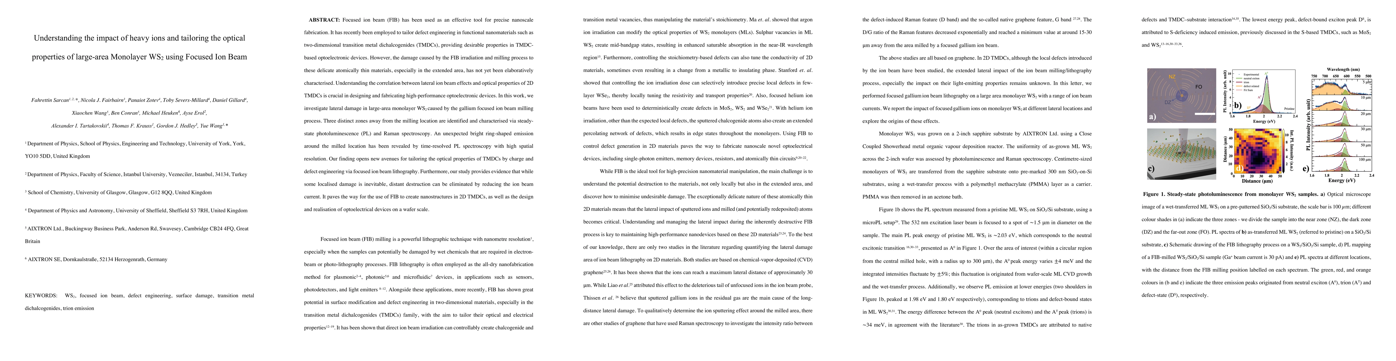
Focused ion beam (FIB) has been used as an effective tool for precise nanoscale fabrication. It has recently been employed to tailor defect engineering in functional nanomaterials such as two-dimens...
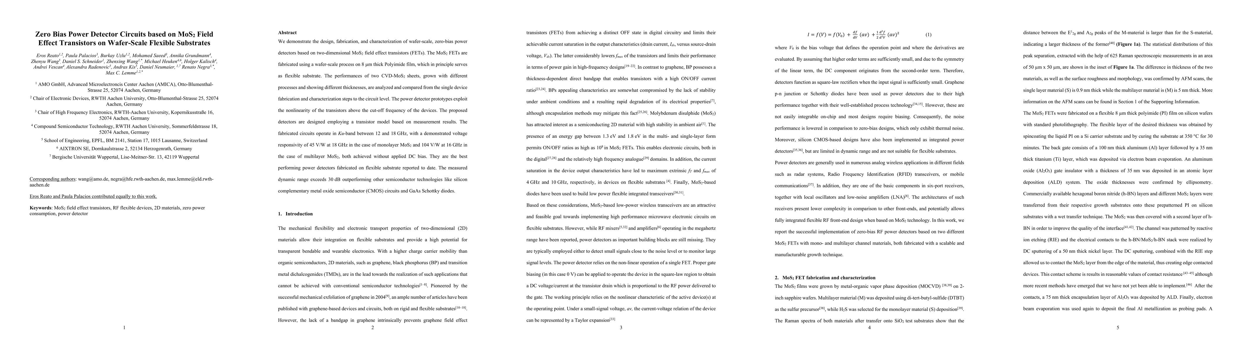
We demonstrate the design, fabrication, and characterization of wafer-scale, zero-bias power detectors based on two-dimensional MoS$_2$ field effect transistors (FETs). The MoS$_2$ FETs are fabricat...
This paper reviews recent progress and key challenges in process and reliability for high-performance vertical GaN transistors and diodes, focusing on the 200 mm CMOS-compatible technology. We parti...
A reliable and scalable transfer of 2D-TMDCs (two-dimensional transition metal dichalcogenides) from the growth substrate to a target substrate with high reproducibility and yield is a crucial step fo...
Layered two-dimensional (2D) semiconductors have shown enhanced ion migration capabilities along their van der Waals (vdW) gaps and on their surfaces. This effect can be employed for resistive switchi...
Two-dimensional materials (2DMs) have been widely investigated because of their potential for heterogeneous integration with modern electronics. However, several major challenges remain, such as the d...
A method for assessing the quality of electronic material properties of thin-film metal oxide semiconductor field-effect transistors (MOSFETs) is presented. By investigating samples with MOCVD-grown M...
Two-dimensional material (2DM)-based field-effect transistors (FETs), such as molybdenum disulfide (MoS${_2}$)-FETs, have gained significant attention for their potential for ultra-short channels, the...
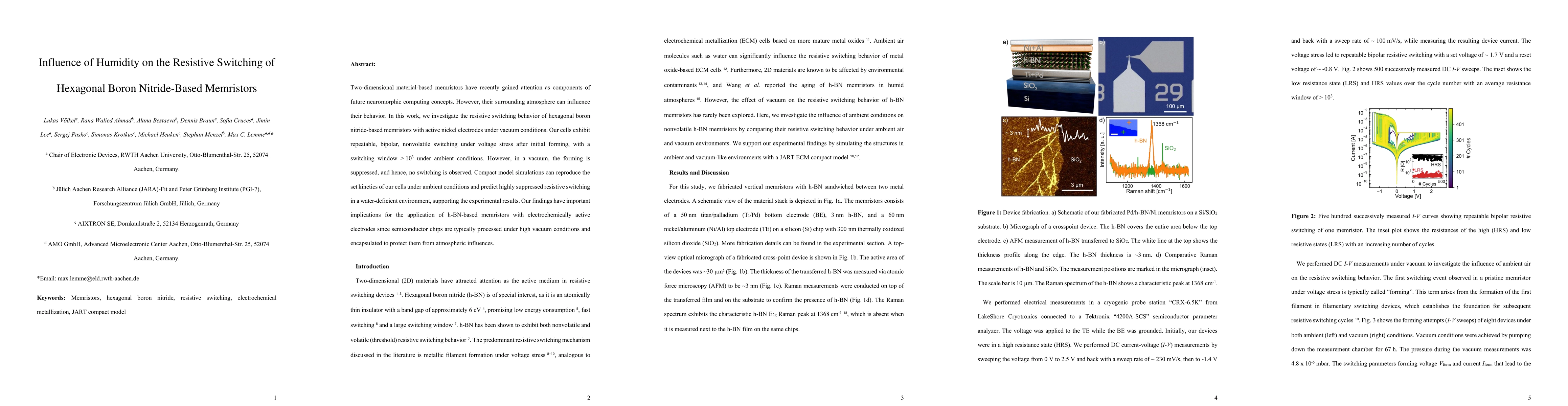
Two-dimensional material-based memristors have recently gained attention as components of future neuromorphic computing concepts. However, their surrounding atmosphere can influence their behavior. In...
Developing electronic devices capable of emulating biological functions is essential for advancing brain-inspired computation paradigms such as neuromorphic computing. In recent years, two-dimensional...
Memristors based on two-dimensional materials (2DMs) have garnered significant attention due to their fast resistive switching (RS) behavior and atomic-level thickness, which enables low power consump...