ArxivLens
M
Researcher

Michael Waltl

8 papers on arXiv

8 arXiv Papers
170 Total Publications
Profile

Academic Profile

Name M. Waltl
Total Papers 170
Scholar Profile View on Semantic Scholar
Metrics

Statistics

8 arXiv Papers
170 Total Publications
Publications

Papers on arXiv

Thumbnail for Time-Gated Optical Spectroscopy of Field-Effect Stimulated Recombination
  via Interfacial Point Defects in Fully-Processed Silicon Carbide Power
  MOSFETs
arXiv
Time-Gated Optical Spectroscopy of Field-Effect Stimulated Recombination via Interfacial Point Defects in Fully-Processed Silicon Carbide Power MOSFETs

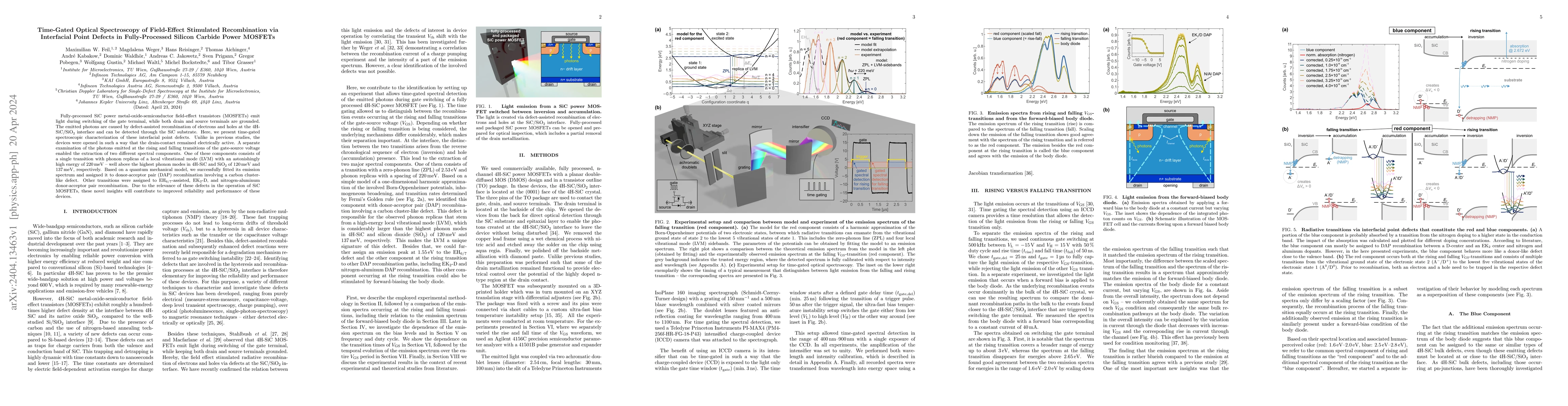
Fully-processed SiC power metal-oxide-semiconductor field-effect transistors (MOSFETs) emit light during switching of the gate terminal, while both drain and source terminals are grounded. The emitt...

Thumbnail for Variability and Reliability of Graphene Field-Effect Transistors with
  CaF2 Insulators
arXiv
Variability and Reliability of Graphene Field-Effect Transistors with CaF2 Insulators

Graphene is a promising material for applications as a channel in graphene field-effect transistors (GFETs) which may be used as a building block for optoelectronics, high-frequency devices and sens...

Thumbnail for Comphy v3.0 -- A Compact-Physics Framework for Modeling Charge Trapping
  Related Reliability Phenomena in MOS Devices
arXiv
Comphy v3.0 -- A Compact-Physics Framework for Modeling Charge Trapping Related Reliability Phenomena in MOS Devices

Charge trapping plays an important role for the reliability of electronic devices and manifests itself in various phenomena like bias temperature instability (BTI), random telegraph noise (RTN), hys...

Thumbnail for Optimizing the Stability of FETs Based on Two-Dimensional Materials by
  Fermi Level Tuning
arXiv
Optimizing the Stability of FETs Based on Two-Dimensional Materials by Fermi Level Tuning

Despite the enormous progress achieved during the past decade, nanoelectronic devices based on two-dimensional (2D) semiconductors still suffer from a limited electrical stability. This limited stab...

Thumbnail for On the suitability of hBN as an insulator for 2D material-based
  ultrascaled CMOS devices
arXiv
On the suitability of hBN as an insulator for 2D material-based ultrascaled CMOS devices

Complementary metal oxide semiconductor (CMOS) logic circuits at the ultimate scaling limit place the utmost demands on the properties of all materials involved. The requirements for semiconductors ...

Thumbnail for Investigation of Low Frequency Noise in CryoCMOS devices through
  Statistical Single Defect Spectroscopy
arXiv
Investigation of Low Frequency Noise in CryoCMOS devices through Statistical Single Defect Spectroscopy

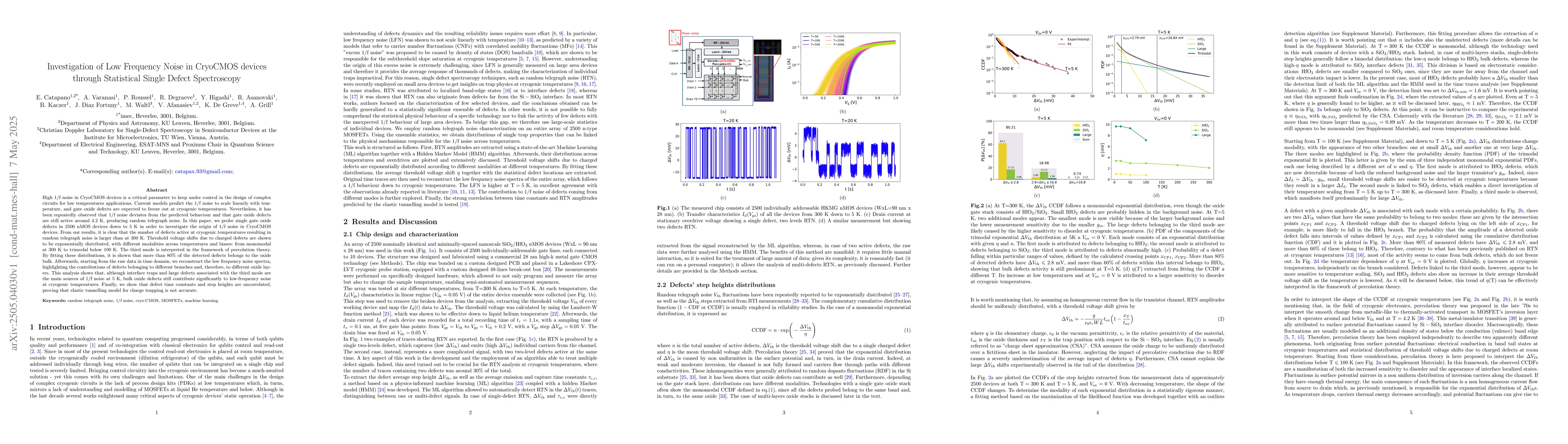
High 1/f noise in CryoCMOS devices is a critical parameter to keep under control in the design of complex circuits for low temperatures applications. Current models predict the 1/f noise to scale line...

Thumbnail for Influence of the Effective Mass on ab initio Phonon-limited Electron
  Mobility of GaAs
arXiv
Influence of the Effective Mass on ab initio Phonon-limited Electron Mobility of GaAs

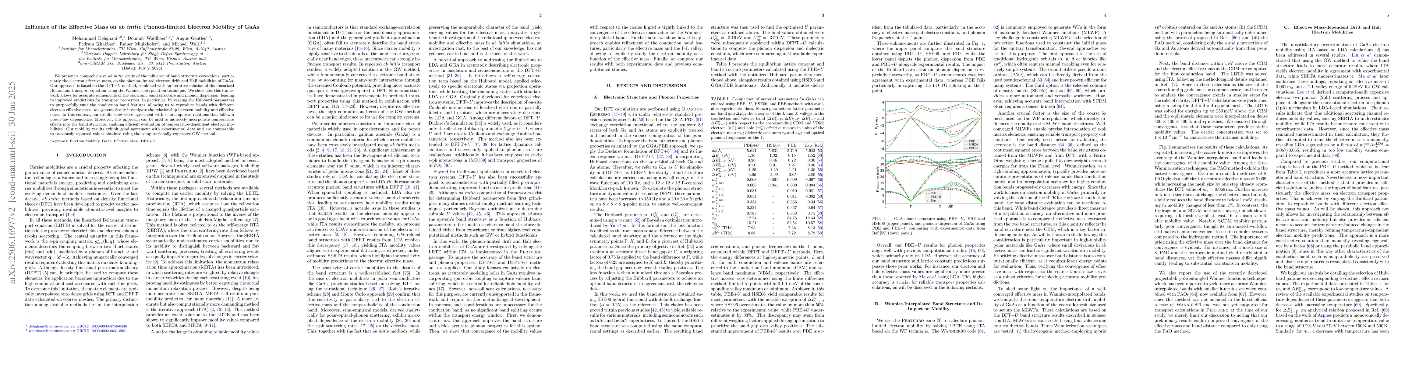
We present a comprehensive ab initio study of the influence of band structure corrections, particularly the electron effective mass, on the phonon-limited electron drift and Hall mobilities of GaAs. O...

Thumbnail for Hysteresis Measurements as a Diagnostic Tool: A Systematic Approach for
  Stability Benchmarking and Performance Projection of 2D-Materials-Based
  MOSFETs
arXiv
Hysteresis Measurements as a Diagnostic Tool: A Systematic Approach for Stability Benchmarking and Performance Projection of 2D-Materials-Based MOSFETs

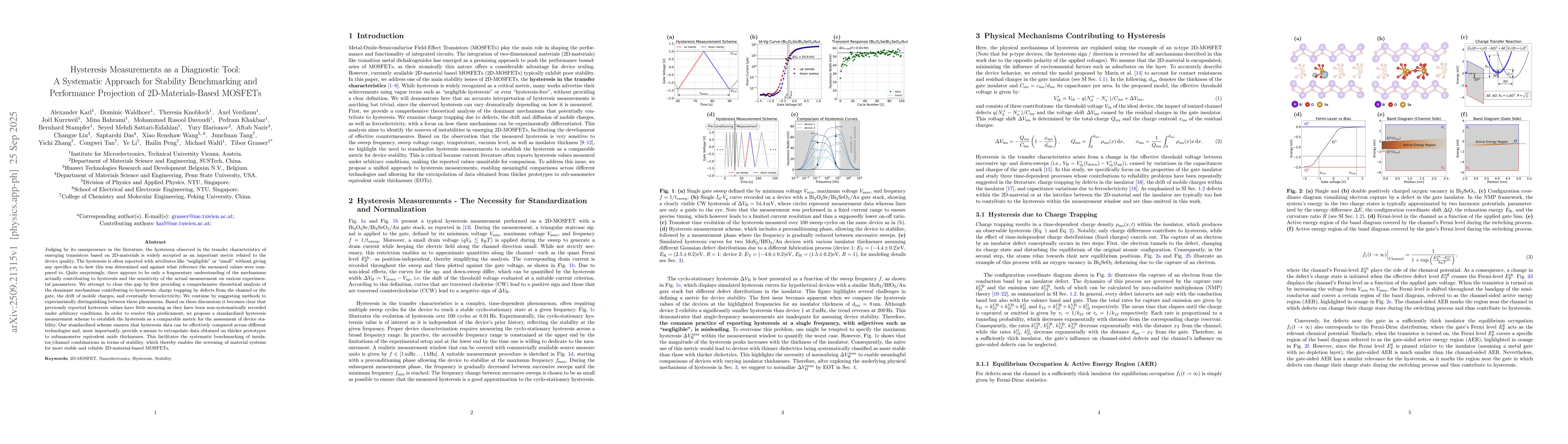
Judging by its omnipresence in the literature, the hysteresis observed in the transfer characteristics of emerging transistors based on 2D-materials is widely accepted as an important metric related t...

This website uses cookies to ensure you get the best experience. Learn more