Academic Profile
Statistics
Similar Authors
Papers on arXiv
As a burgeoning technique, out-of-focus electron ptychography offers the potential for rapidly imaging atomic-scale large fields of view (FoV) using a single diffraction dataset. However, achieving ...
Correcting scan-positional errors is critical in achieving electron ptychography with both high resolution and high precision. This is a demanding and challenging task due to the sheer number of par...
Two-dimensional (2D) semiconductors are promising channel materials for continued downscaling of complementary metal-oxide-semiconductor (CMOS) logic circuits. However, their full potential continue...
Phase change memory devices are typically reset by melt-quenching a material to radically lower its electrical conductance. The high power and concomitantly high current density required to reset ph...
Three-dimensional (3D) imaging of thin, extended specimens at nanometer resolution is critical for applications in biology, materials science, advanced synthesis, and manufacturing. One route to 3D ...
The switchable optical and electrical properties of phase change materials (PCMs) are finding new applications beyond data storage in reconfigurable photonic devices. However, high power heat pulses...
Chalcogenide phase change materials (PCMs) have been extensively applied in data storage, and they are now being proposed for high resolution displays, holographic displays, reprogrammable photonics...
Bound-states-in-the-continuum (BIC)is a wave-mechanical concept that generates resonances with vanishing spectral linewidths. It has many practical applications in Optics, such as narrow-band filter...
The accurate determination of the compositional fluctuations is pivotal in understanding their role in the reduction of efficiency in high indium content $In_{x}Ga_{1-x}N$ light-emitting diodes, the...
We introduce a new mechanism for second-harmonic generation through geometrically rectifying-funneling-ballistic electrons in THz optical resonators. Our resonant rectifiers inherently act as second-o...
Extreme light confinement down to the atomic scale has been theoretically predicted for ultrathin, Ta-based transition metal dichalcogenides (TMDs). In this work, we demonstrate in free-hanging 2H-TaS...
Two-dimensional van der Waals semiconductors are promising for future nanoelectronics. However, integrating high-k gate dielectrics for device applications is challenging as the inert van der Waals ma...
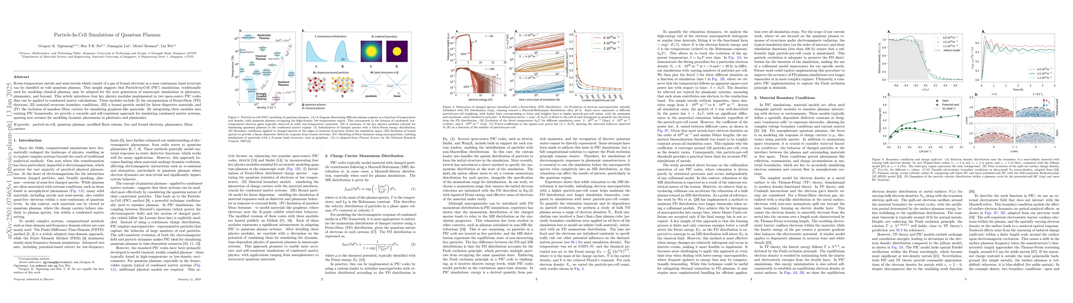
Room-temperature metals and semi-metals which consist of a gas of bound electrons in a near-continuum band structure can be classified as cold quantum plasmas. This insight suggests that Particle-in-C...
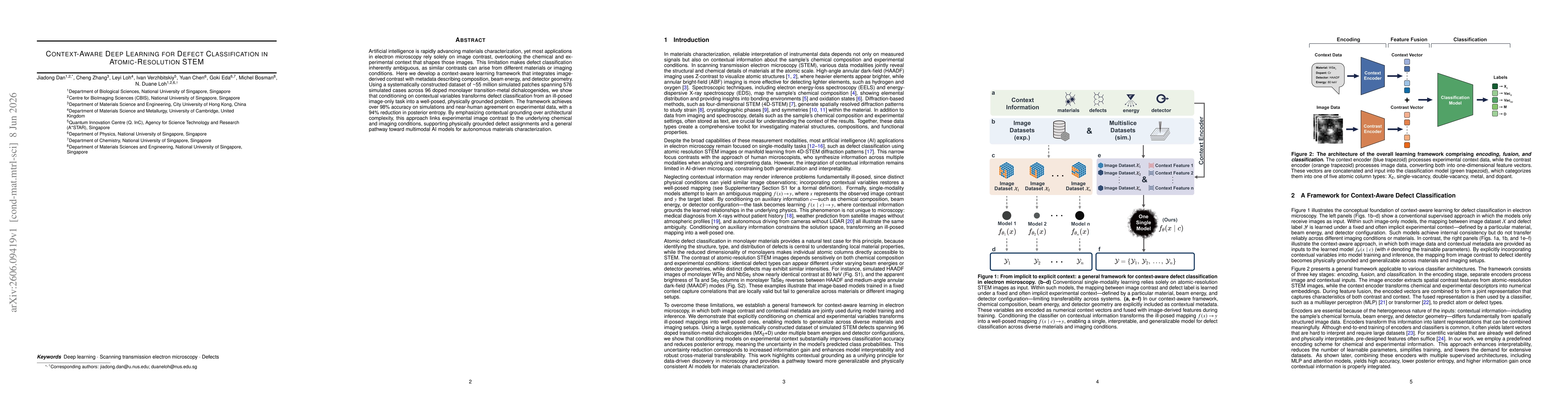
Artificial intelligence is rapidly advancing materials characterization, yet most applications in electron microscopy rely solely on image contrast, overlooking the chemical and experimental context t...
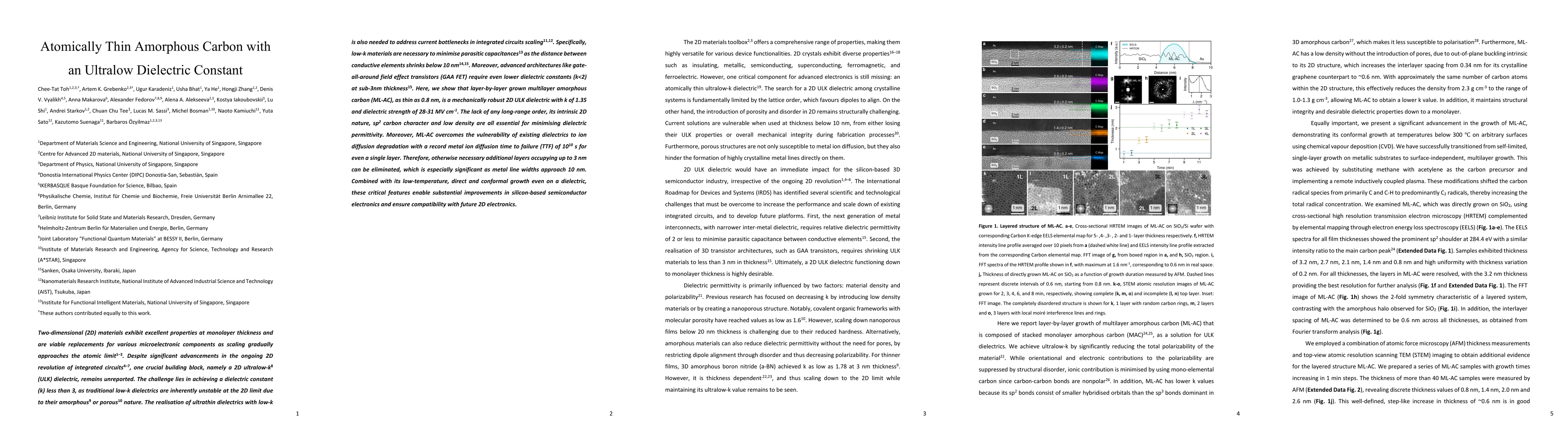
Two-dimensional (2D) materials exhibit excellent properties at monolayer thickness and are viable replacements for various microelectronic components as scaling gradually approaches the atomic limit. ...
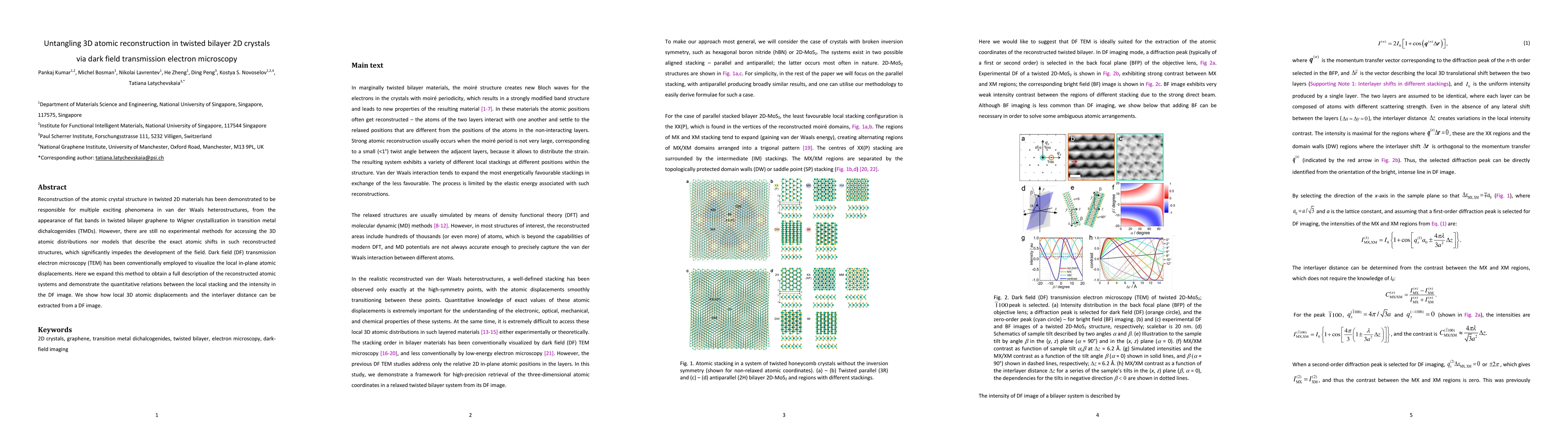
Reconstruction of the atomic crystal structure in twisted 2D materials has been demonstrated to be responsible for multiple exciting phenomena in van der Waals heterostructures, from the appearance of...