Mihail Ion Lepsa

7 papers on arXiv

Academic Profile

Name: M. Lepsa
Total Papers: 69

Statistics

arXiv Papers 7
Total Publications 69

Papers on arXiv

Thumbnail for Semiconductor membranes for electrostatic exciton trapping in optically
  addressable quantum transport devices

Semiconductor membranes for electrostatic exciton trapping in optically addressable quantum transport devices

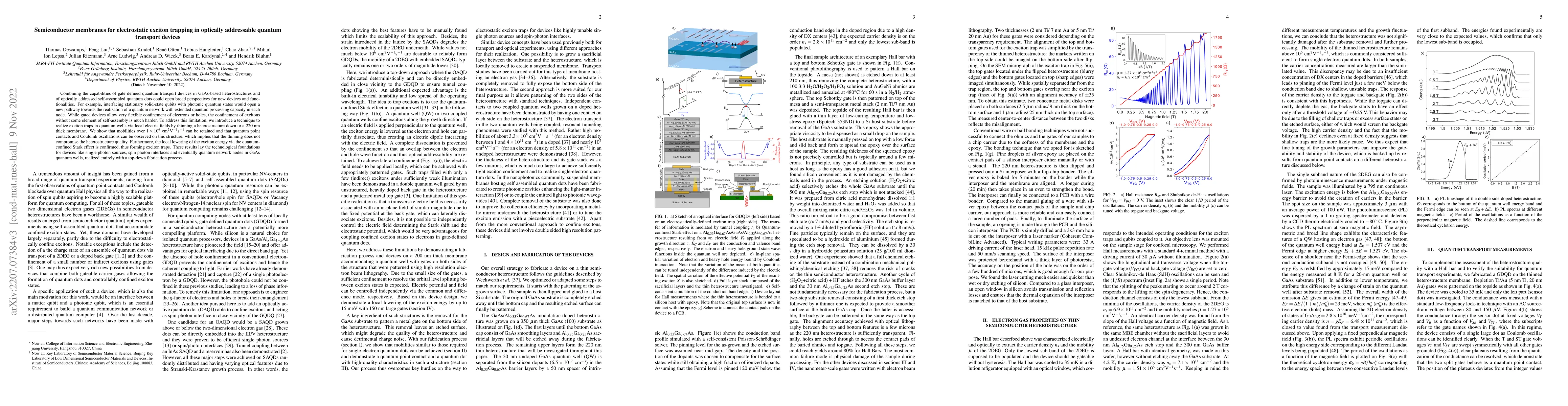
Combining the capabilities of gate defined quantum transport devices in GaAs-based heterostructures and of optically addressed self-assembled quantum dots could open broad perspectives for new devic...

Thumbnail for Microwave spectroscopy of Andreev states in InAs nanowire-based hybrid
  junctions using a flip-chip layout

Microwave spectroscopy of Andreev states in InAs nanowire-based hybrid junctions using a flip-chip layout

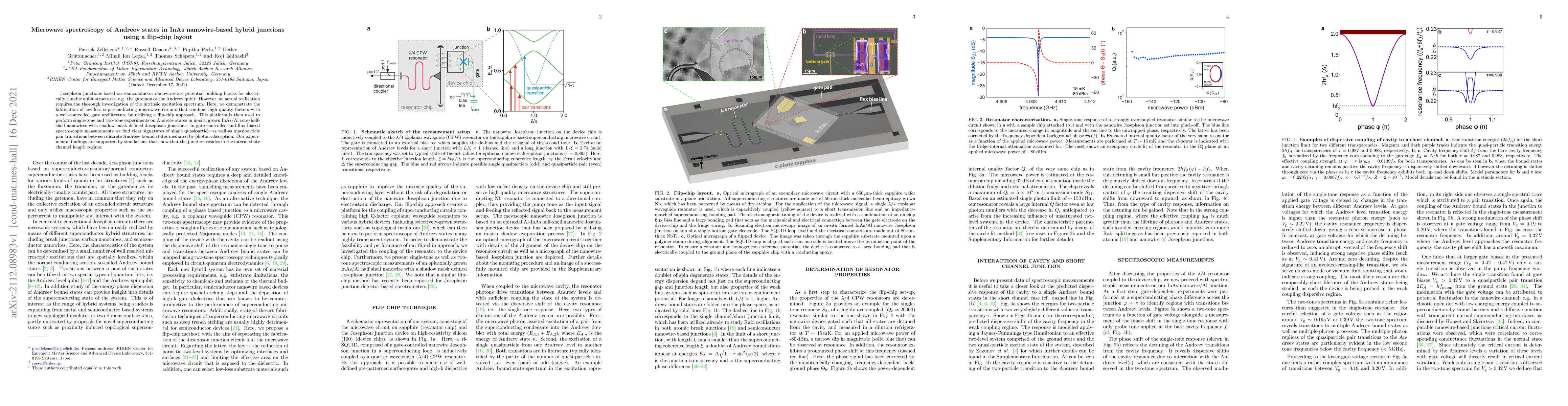
Josephson junctions based on semiconductor nanowires are potential building blocks for electrically tunable qubit structures, e.g. the gatemon or the Andreev qubit. However, an actual realization re...

Thumbnail for Te-doped selective-area grown InAs nanowires for superconducting hybrid
  devices

Te-doped selective-area grown InAs nanowires for superconducting hybrid devices

Semiconductor nanowires have emerged as versatile components in superconducting hybrid devices for Majorana physics and quantum computing. The transport properties of nanowires can be tuned either b...

Thumbnail for Fully in-situ InAs nanowire Josephson junctions by selective-area growth
  and shadow evaporation

Fully in-situ InAs nanowire Josephson junctions by selective-area growth and shadow evaporation

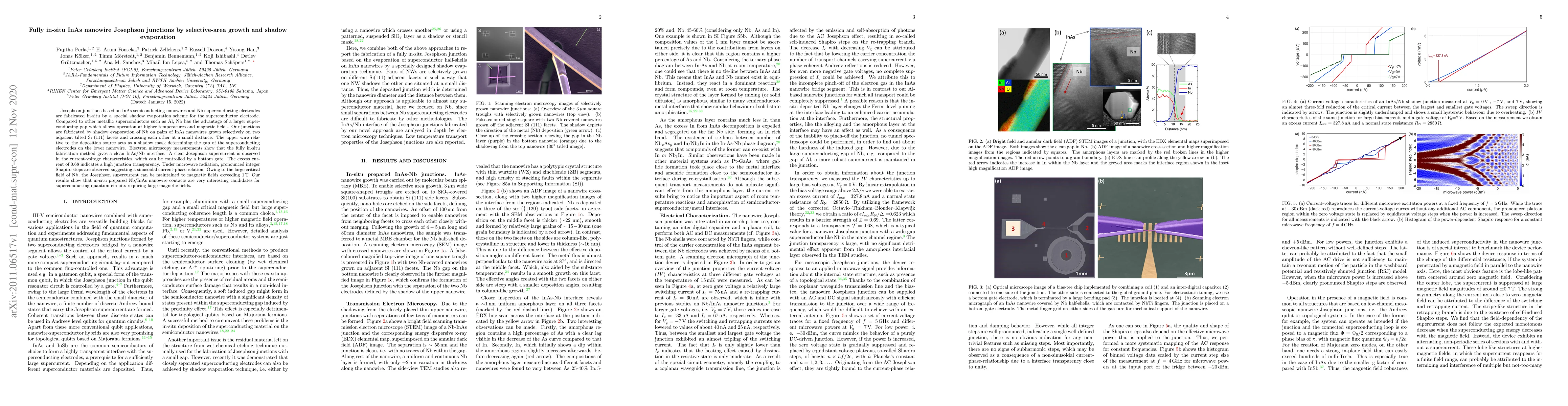
Josephson junctions based on InAs semiconducting nanowires and Nb superconducting electrodes are fabricated in-situ by a special shadow evaporation scheme for the superconductor electrode. Compared ...

Thumbnail for Influence of Te-doping on self-catalyzed VS InAs nanowires

Influence of Te-doping on self-catalyzed VS InAs nanowires

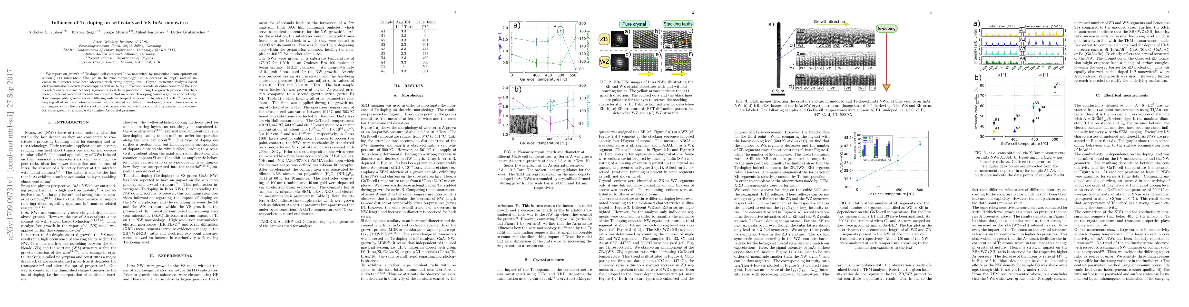
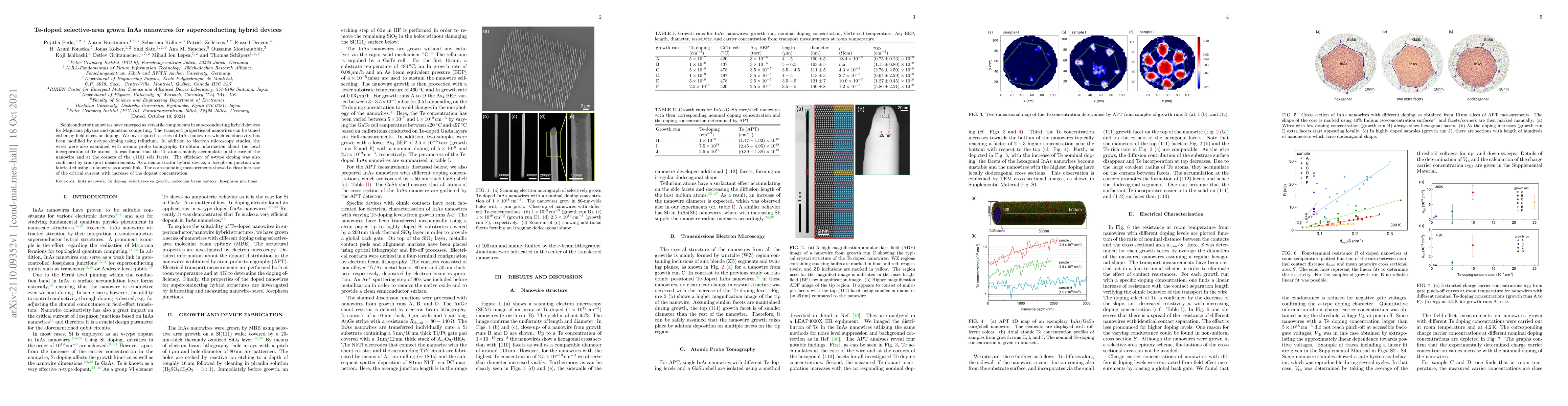
We report on growth of Te-doped self-catalyzed InAs nanowires by molecular beam epitaxy on silicon (111) substrates. Changes in the wire morphology, i.e. a decrease in length and an increase in diam...

Thumbnail for MBE Growth of Al/InAs and Nb/InAs Superconducting Hybrid Nanowire
  Structures

MBE Growth of Al/InAs and Nb/InAs Superconducting Hybrid Nanowire Structures

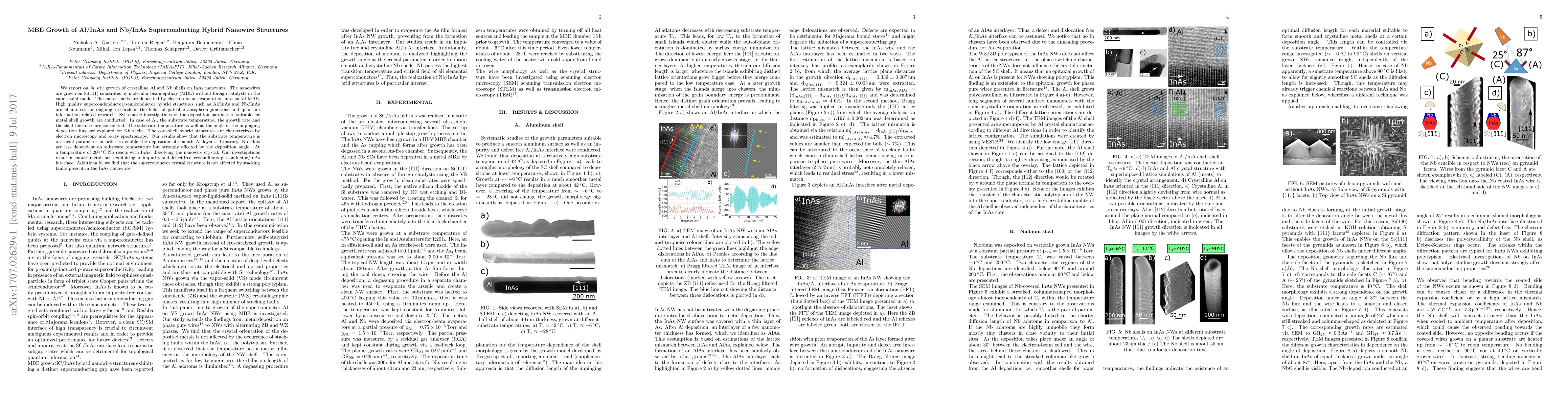
We report on \textit{in situ} growth of crystalline Al and Nb shells on InAs nanowires. The nanowires are grown on Si(111) substrates by molecular beam epitaxy (MBE) without foreign catalysts in the...

Thumbnail for Fabrication and characterization of InAs nanowire-based quantum dot
  structures utilizing buried bottom gates

Fabrication and characterization of InAs nanowire-based quantum dot structures utilizing buried bottom gates

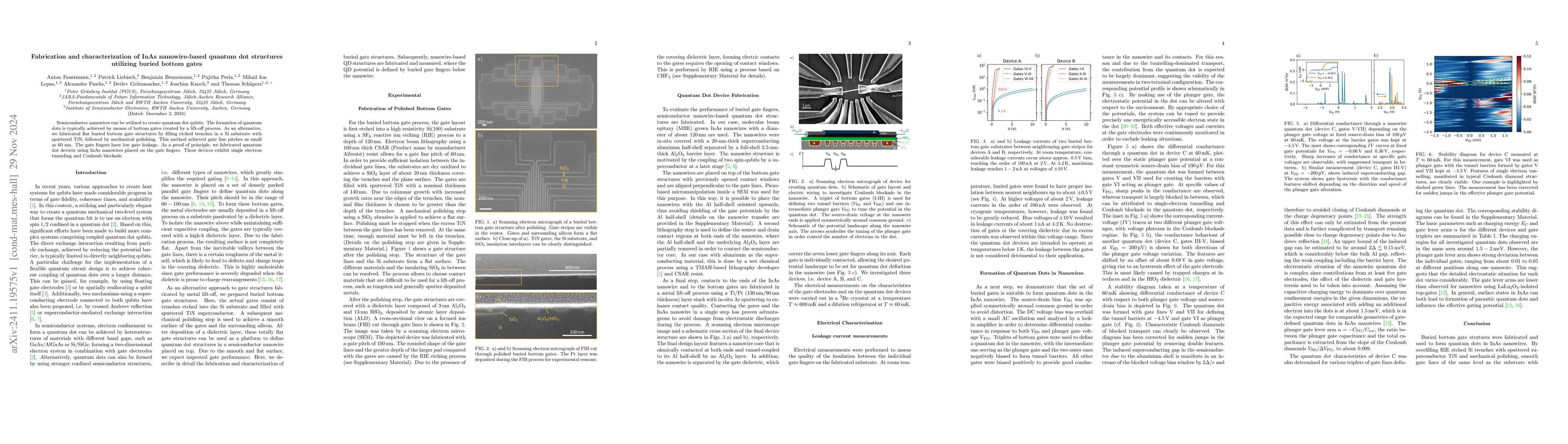
Semiconductor nanowires can be utilized to create quantum dot qubits. The formation of quantum dots is typically achieved by means of bottom gates created by a lift-off process. As an alternative, we ...

This website uses cookies to ensure you get the best experience. Learn more