Nicholas J. Borys

8 papers on arXiv

Academic Profile

Name: N. Borys
Total Papers: 111

Statistics

arXiv Papers 8
Total Publications 111

Papers on arXiv

Thumbnail for Highly tunable room-temperature plexcitons in monolayer WSe2
  /gap-plasmon nanocavities

Highly tunable room-temperature plexcitons in monolayer WSe2 /gap-plasmon nanocavities

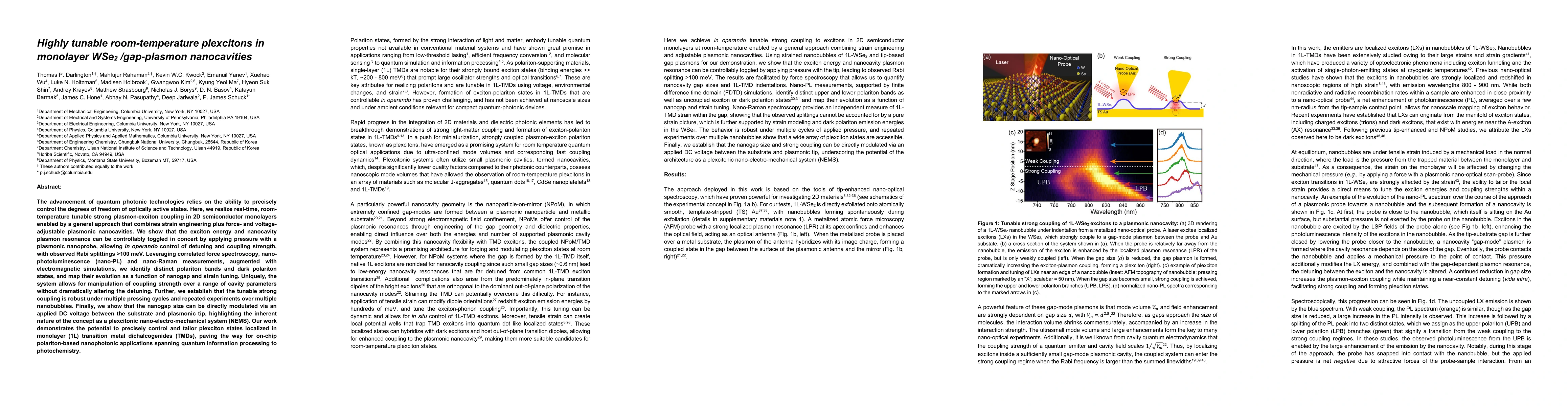
The advancement of quantum photonic technologies relies on the ability to precisely control the degrees of freedom of optically active states. Here, we realize real-time, room-temperature tunable st...

Thumbnail for Programmable Nanowrinkle-Induced Room-Temperature Exciton Localization
  in Monolayer WSe2

Programmable Nanowrinkle-Induced Room-Temperature Exciton Localization in Monolayer WSe2

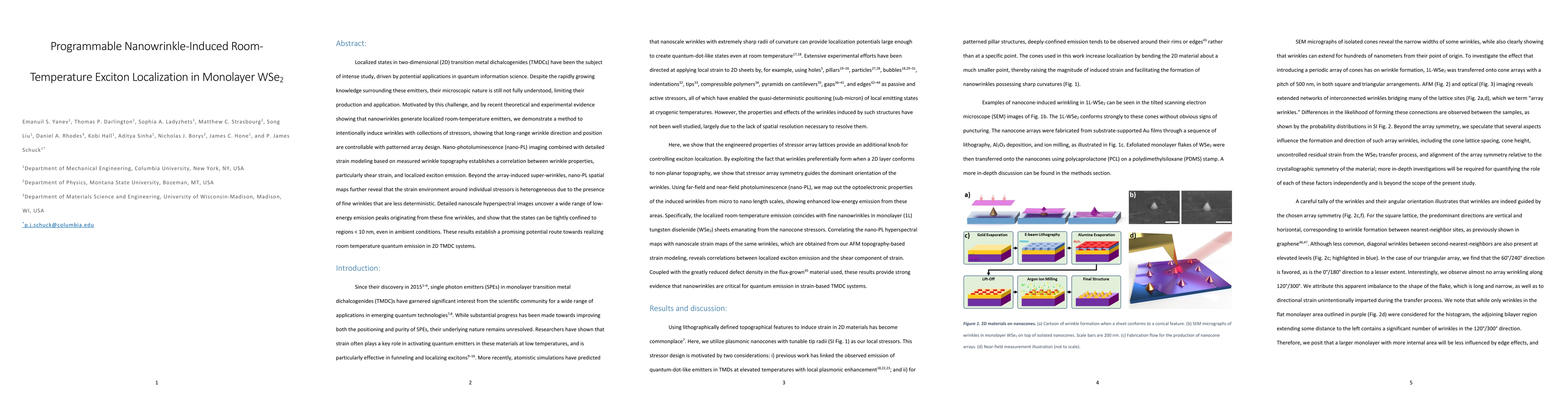
Localized states in two-dimensional (2D) transition metal dichalcogenides (TMDCs) have been the subject of intense study, driven by potential applications in quantum information science. Despite the...

Thumbnail for Direct Nano-Imaging of Light-Matter Interactions in Nanoscale Excitonic
  Emitters

Direct Nano-Imaging of Light-Matter Interactions in Nanoscale Excitonic Emitters

Strong light-matter interactions in localized nano-emitters when placed near metallic mirrors have been widely reported via spectroscopic studies in the optical far-field. Here, we report a near-fie...

Thumbnail for Nanoscale Raman Characterization of a 2D Semiconductor Lateral
  Heterostructure Interface

Nanoscale Raman Characterization of a 2D Semiconductor Lateral Heterostructure Interface

The nature of the interface in lateral heterostructures of 2D monolayer semiconductors including its composition, size, and heterogeneity critically impacts the functionalities it engenders on the 2...

Thumbnail for How Substitutional Point Defects in Two-Dimensional WS$_2$ Induce Charge
  Localization, Spin-Orbit Splitting, and Strain

How Substitutional Point Defects in Two-Dimensional WS$_2$ Induce Charge Localization, Spin-Orbit Splitting, and Strain

Control of impurity concentrations in semiconducting materials is essential to device technology. Because of their intrinsic confinement, the properties of two-dimensional semiconductors such as tra...

Thumbnail for Planar Aperiodic Arrays as Metasurfaces for Optical Near-Field
  Patterning

Planar Aperiodic Arrays as Metasurfaces for Optical Near-Field Patterning

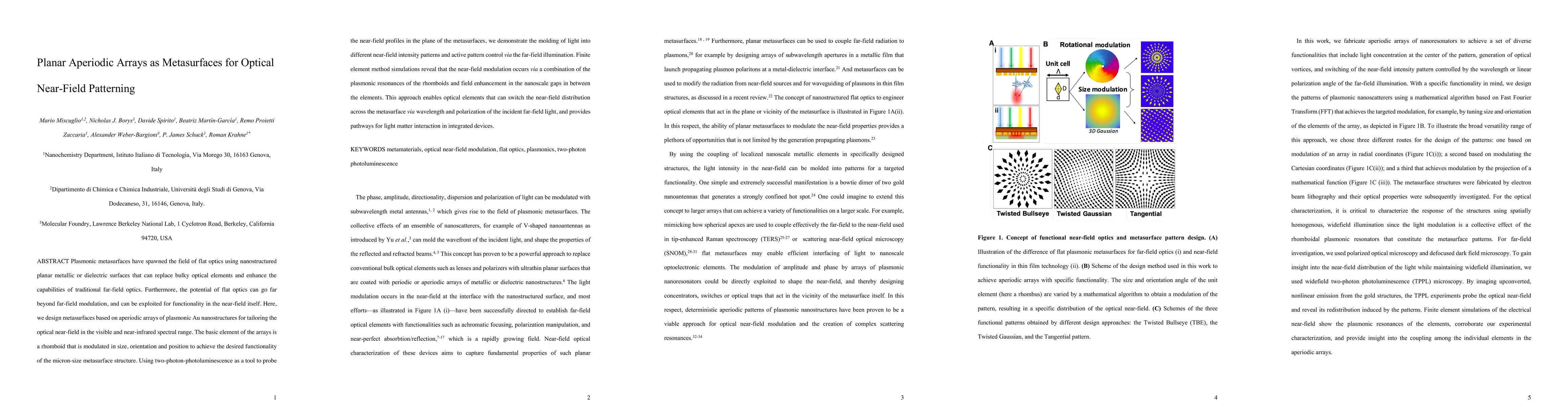
Plasmonic metasurfaces have spawned the field of flat optics using nanostructured planar metallic or dielectric surfaces that can replace bulky optical elements and enhance the capabilities of tradi...

Thumbnail for Imaging strain-localized exciton states in nanoscale bubbles in
  monolayer WSe2 at room temperature

Imaging strain-localized exciton states in nanoscale bubbles in monolayer WSe2 at room temperature

In monolayer transition metal dichalcogenides, quantum emitters are associated with localized strain that can be deterministically applied to create designer nano-arrays of single photon sources. De...

Thumbnail for The ultrafast onset of exciton formation in 2D semiconductors

The ultrafast onset of exciton formation in 2D semiconductors

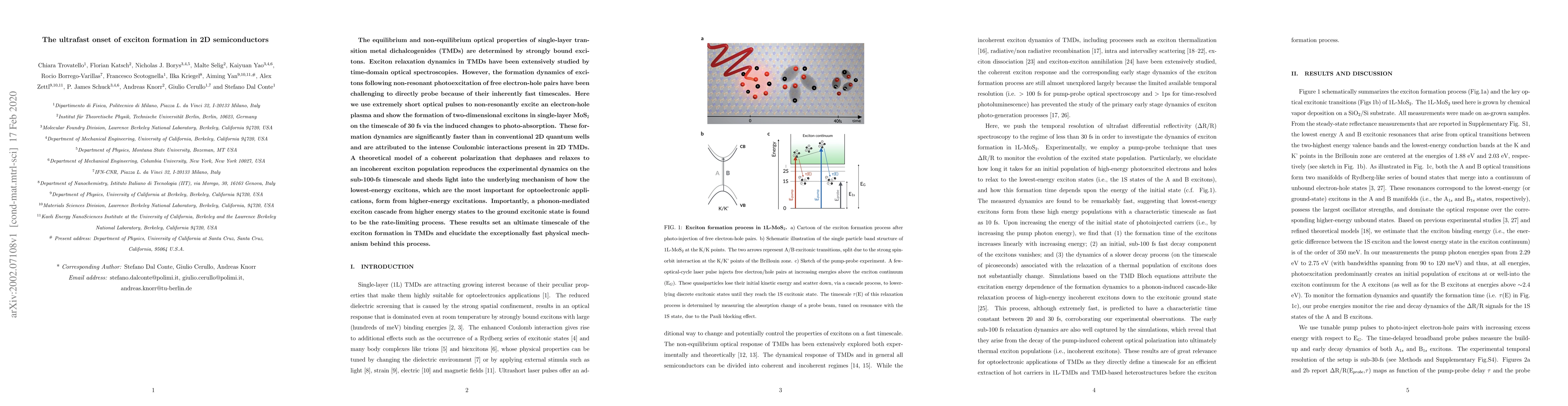
The equilibrium and non-equilibrium optical properties of single-layer transition metal dichalcogenides (TMDs) are determined by strongly bound excitons. Exciton relaxation dynamics in TMDs have bee...

This website uses cookies to ensure you get the best experience. Learn more