ArxivLens
O
Researcher

Oliver Bierwagen

24 papers on arXiv

24 arXiv Papers
3 Total Publications
Profile

Academic Profile

Name O. Bierwagen
Total Papers 3
Scholar Profile View on Semantic Scholar
Metrics

Statistics

24 arXiv Papers
3 Total Publications
Publications

Papers on arXiv

Thumbnail for Etching of elemental layers in oxide molecular beam epitaxy by
  O2-assisted formation and evaporation of their volatile suboxide: The
  examples of Ga and Ge
arXiv
Etching of elemental layers in oxide molecular beam epitaxy by O2-assisted formation and evaporation of their volatile suboxide: The examples of Ga and Ge

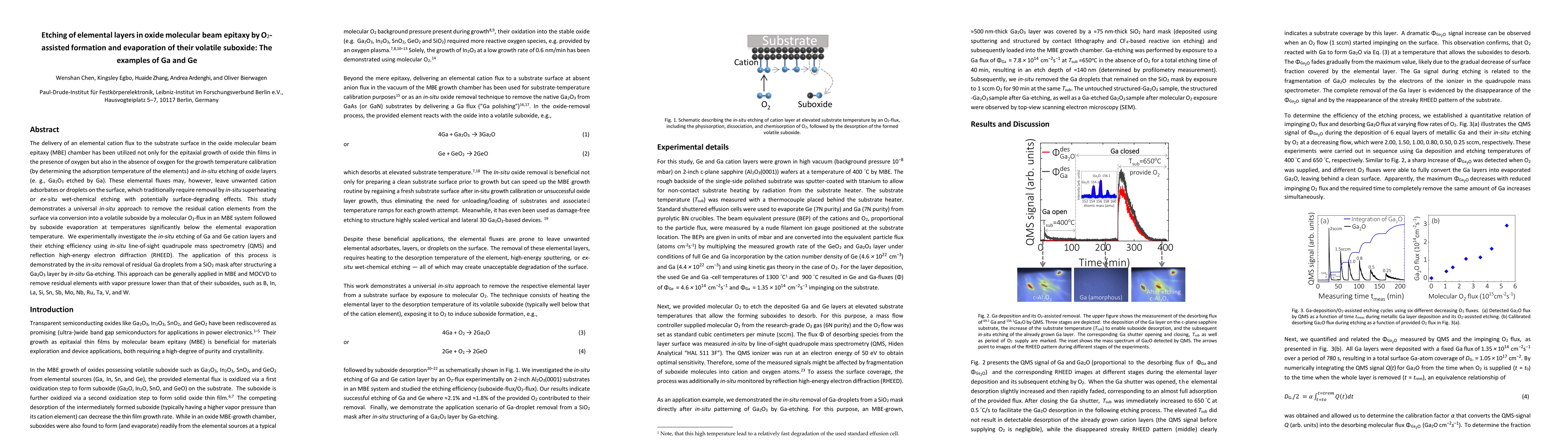
The delivery of an elemental cation flux to the substrate surface in the oxide molecular beam epitaxy (MBE) chamber has been utilized not only for the epitaxial growth of oxide thin films in the pre...

Thumbnail for In-situ study and modeling of the reaction kinetics during molecular
  beam epitaxy of GeO2 and its etching by Ge
arXiv
In-situ study and modeling of the reaction kinetics during molecular beam epitaxy of GeO2 and its etching by Ge

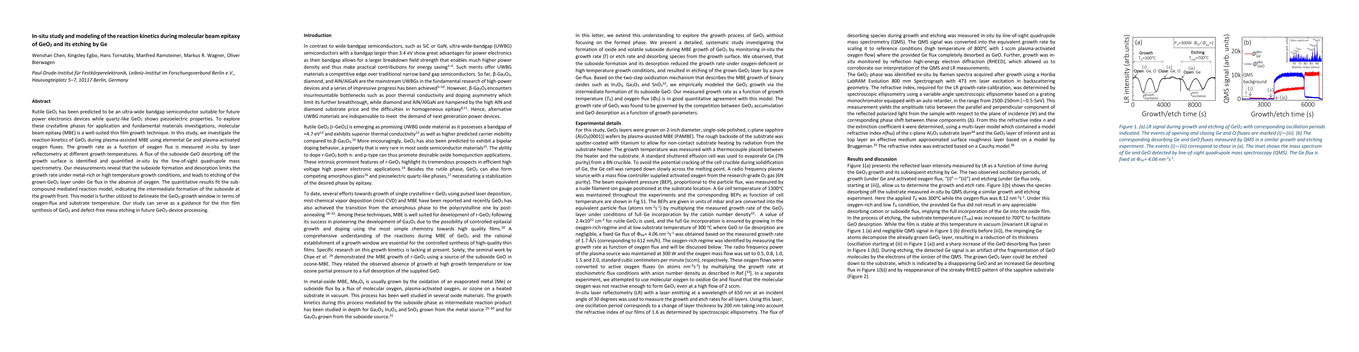
Rutile GeO2 has been predicted to be an ultra-wide bandgap semiconductor suitable for future power electronics devices while quartz-like GeO2 shows piezoelectric properties. To explore these crystal...

Thumbnail for Adsorption-controlled plasma-assisted molecular beam epitaxy of LaInO3
  on DyScO3(110): Growth window, strain relaxation, and domain pattern
arXiv
Adsorption-controlled plasma-assisted molecular beam epitaxy of LaInO3 on DyScO3(110): Growth window, strain relaxation, and domain pattern

We report the growth of epitaxial LaInO3 on DyScO3(110) substrates by adsorption-controlled plasma-assisted molecular beam epitaxy (PA-MBE). The adsorption-controlled growth was monitored using line...

Thumbnail for Acceptor and compensating donor doping of single crystalline SnO (001)
  films grown by molecular beam epitaxy and its perspectives for
  optoelectronics and gas-sensing
arXiv
Acceptor and compensating donor doping of single crystalline SnO (001) films grown by molecular beam epitaxy and its perspectives for optoelectronics and gas-sensing

(La and Ga)-doped tin monoxide (stannous oxide, tin (II) oxide, SnO) thin films were grown by plasma-assisted and suboxide molecular beam epitaxy with dopant concentrations ranging from $\approx5\ti...

Thumbnail for Epitaxial synthesis of unintentionally doped p-type SnO (001) via
  suboxide molecular beam epitaxy
arXiv
Epitaxial synthesis of unintentionally doped p-type SnO (001) via suboxide molecular beam epitaxy

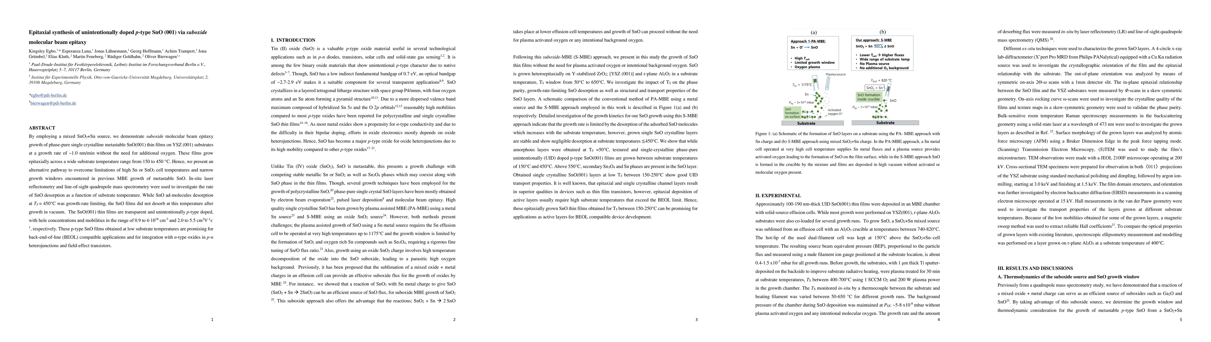
By employing a mixed SnO$_2$+Sn source, we demonstrate suboxide molecular beam epitaxy growth of phase-pure single crystalline metastable SnO(001) thin films at a growth rate of ~1.0nm/min without t...

Thumbnail for Tackling Disorder in $\gamma$-Ga$_2$O$_3$
arXiv
Tackling Disorder in $\gamma$-Ga$_2$O$_3$

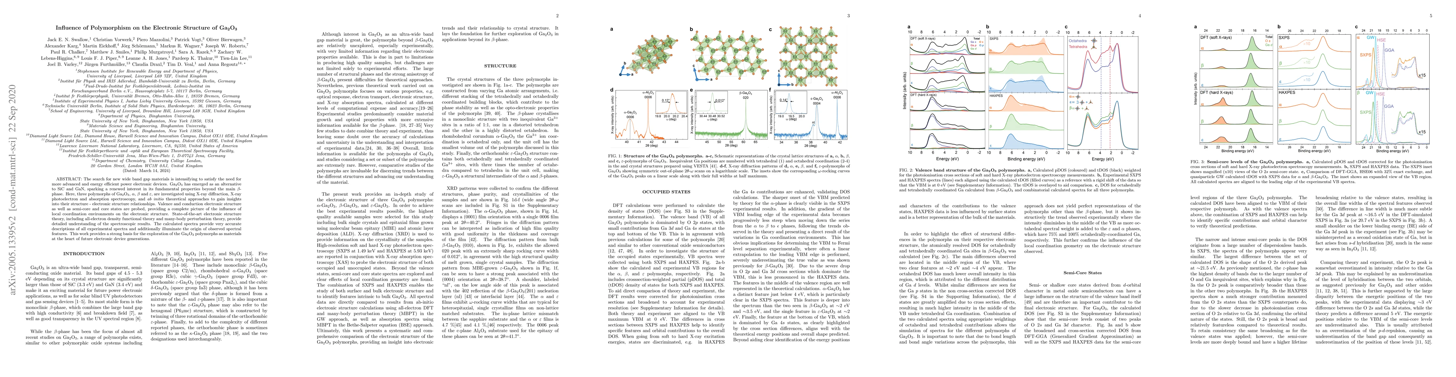
Ga$_2$O$_3$ and its polymorphs are attracting increasing attention. The rich structural space of polymorphic oxide systems such as Ga$_2$O$_3$ offers potential for electronic structure engineering, ...

Thumbnail for The electrical conductivity of cubic (In$_{1-x}$Ga$_x$)$_2$O$_3$ films
  ($x\le0.18$): Native point defects, Sn-doping, and the surface electron
  accumulation layer
arXiv
The electrical conductivity of cubic (In$_{1-x}$Ga$_x$)$_2$O$_3$ films ($x\le0.18$): Native point defects, Sn-doping, and the surface electron accumulation layer

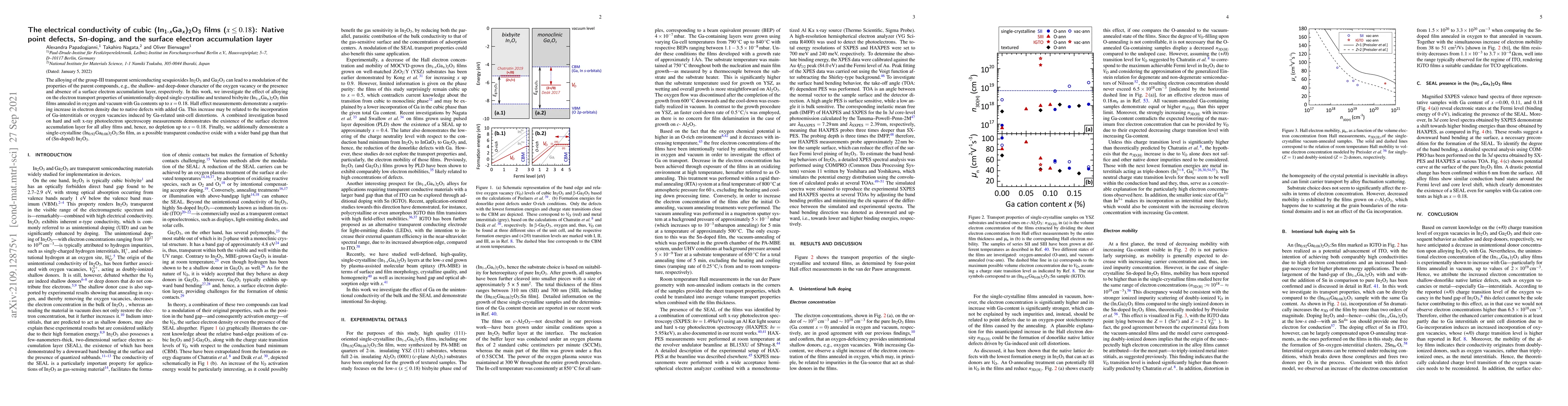
The alloying of the group-III transparent semiconducting sesquioxides In$_2$O$_3$ and Ga$_2$O$_3$ can lead to a modulation of the properties of the parent compounds, e.g., the shallow- and deep-dono...

Thumbnail for Drastically enhanced cation incorporation in the epitaxy of oxides due
  to formation and evaporation of suboxides from elemental sources
arXiv
Drastically enhanced cation incorporation in the epitaxy of oxides due to formation and evaporation of suboxides from elemental sources

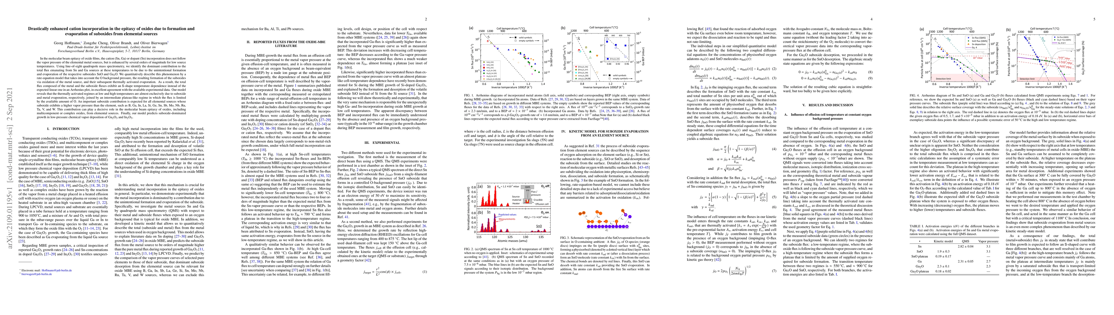
In the molecular beam epitaxy of oxide films, the cation (Sn, Ga) or dopant (Sn) incorporation does not follow the vapor pressure of the elemental metal sources, but is enhanced by several orders of...

Thumbnail for Molecular beam epitaxy of single-crystalline bixbyite
  (In$_{1-x}$Ga$_x$)$_2$O$_3$ films ($x \leq 0.18$): Structural properties and
  consequences of compositional inhomogeneity
arXiv
Molecular beam epitaxy of single-crystalline bixbyite (In$_{1-x}$Ga$_x$)$_2$O$_3$ films ($x \leq 0.18$): Structural properties and consequences of compositional inhomogeneity

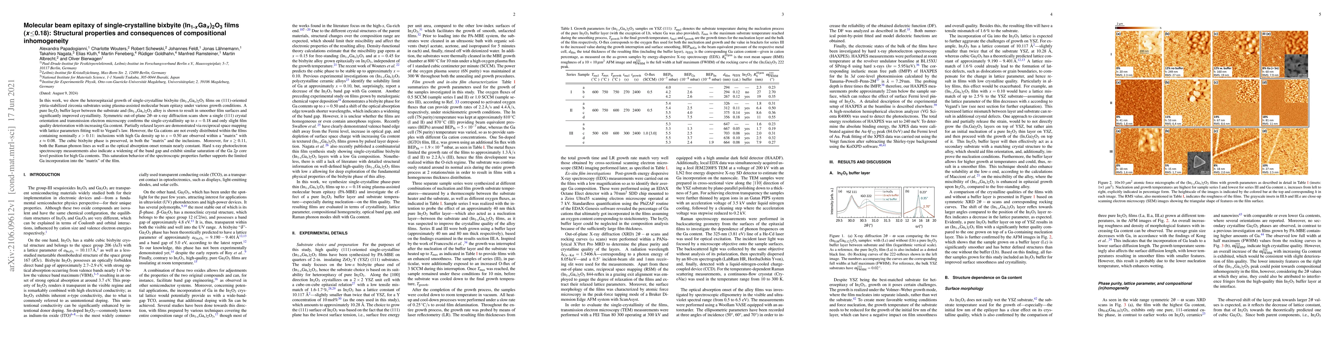
In this work, we show the heteroepitaxial growth of single-crystalline bixbyite (In$_{1-x}$Ga$_x$)$_2$O$_3$ films on (111)-oriented yttria-stabilized zirconia substrates using plasma-assisted molecu...

Thumbnail for Adsorption-Controlled Growth of Ga2O3 by Suboxide Molecular-Beam Epitaxy
arXiv
Adsorption-Controlled Growth of Ga2O3 by Suboxide Molecular-Beam Epitaxy

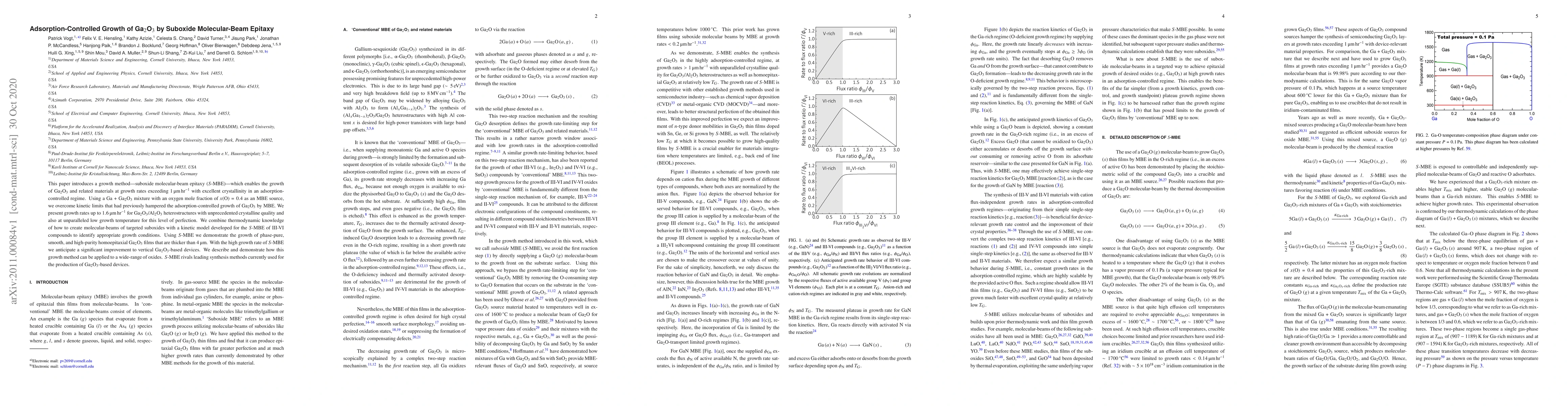
This paper introduces a growth method---suboxide molecular-beam epitaxy (S-MBE)---which enables the growth of Ga2O3 and related materials at growth rates exceeding 1 micrometer per hours with excell...

Thumbnail for Conductance Model for Single-Crystalline/Compact Metal Oxide Gas Sensing
  Layers in the Non-Degenerate Limit: Example of Epitaxial SnO$_2$(101)
arXiv
Conductance Model for Single-Crystalline/Compact Metal Oxide Gas Sensing Layers in the Non-Degenerate Limit: Example of Epitaxial SnO$_2$(101)

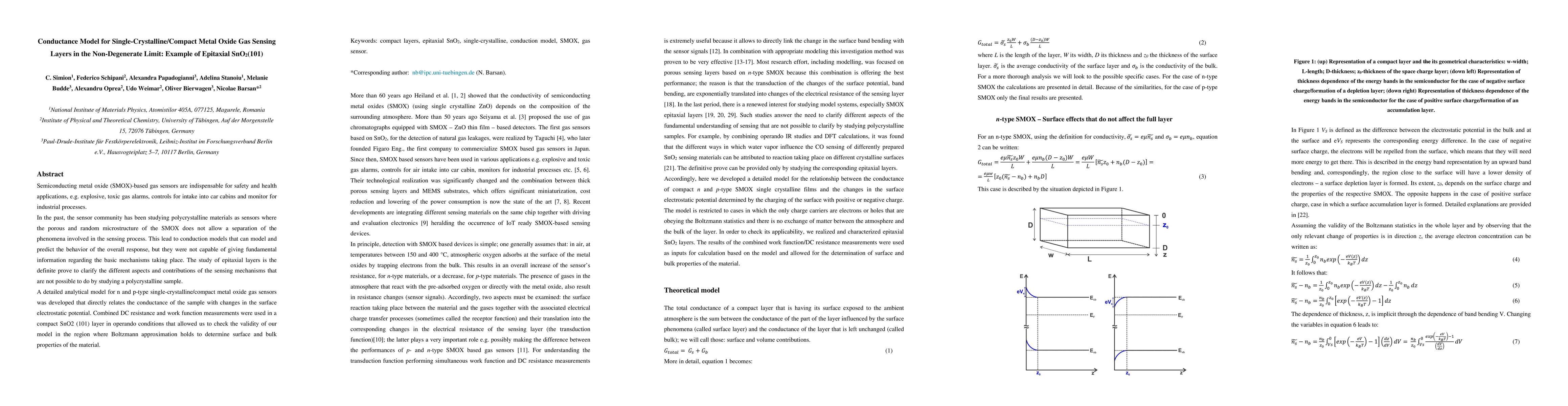
Semiconducting metal oxide (SMOX)-based gas sensors are indispensable for safety and health applications, e.g. explosive, toxic gas alarms, controls for intake into car cabins and monitor for indust...

Thumbnail for Conduction Mechanisms in Epitaxial NiO/Graphene Gas Sensors
arXiv
Conduction Mechanisms in Epitaxial NiO/Graphene Gas Sensors

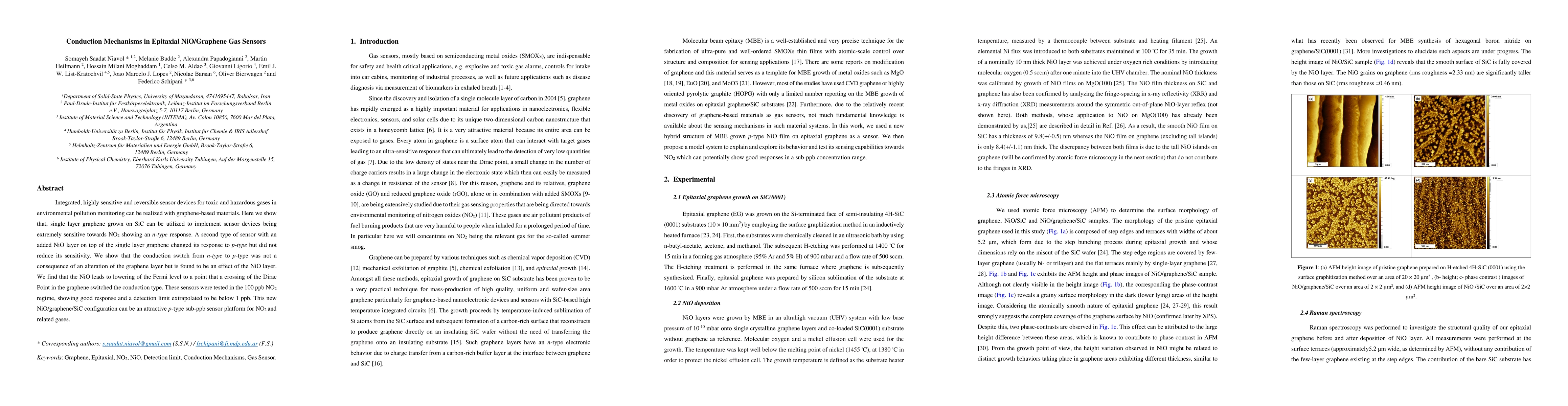
Integrated, highly sensitive and reversible sensor devices for toxic and hazardous gases in environmental pollution monitoring can be realized with graphene-based materials. Here we show that, singl...

Thumbnail for Offcut-related step-flow and growth rate enhancement during (100)
  $\beta$-Ga2O3 homoepitaxy by metal-exchange catalyzed molecular beam epitaxy
  (MEXCAT-MBE)
arXiv
Offcut-related step-flow and growth rate enhancement during (100) $\beta$-Ga2O3 homoepitaxy by metal-exchange catalyzed molecular beam epitaxy (MEXCAT-MBE)

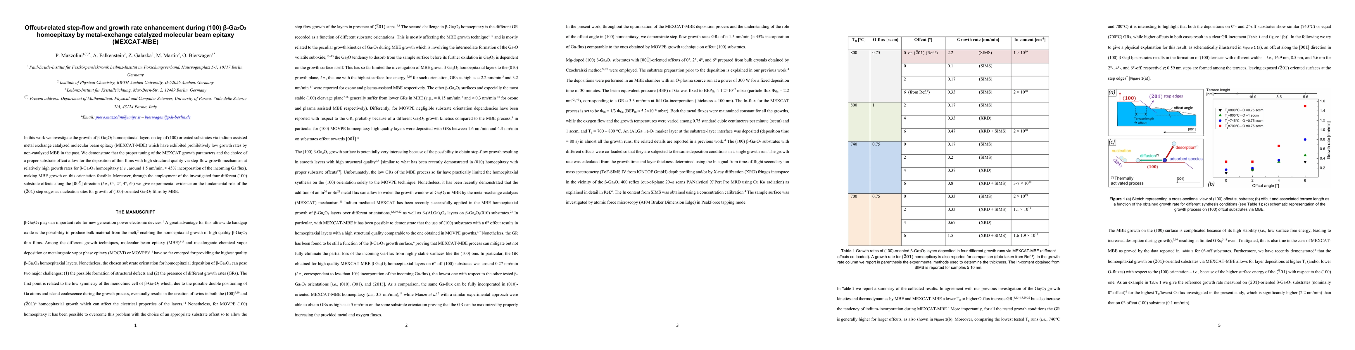
In this work we investigate the growth of $\beta$-Ga2O3 homoepitaxial layers on top of (100) oriented substrates via indium-assisted metal exchange catalyzed molecular beam epitaxy (MEXCAT-MBE) whic...

Thumbnail for SnO/$\beta$-Ga2O3 vertical $pn$ heterojunction diodes
arXiv
SnO/$\beta$-Ga2O3 vertical $pn$ heterojunction diodes

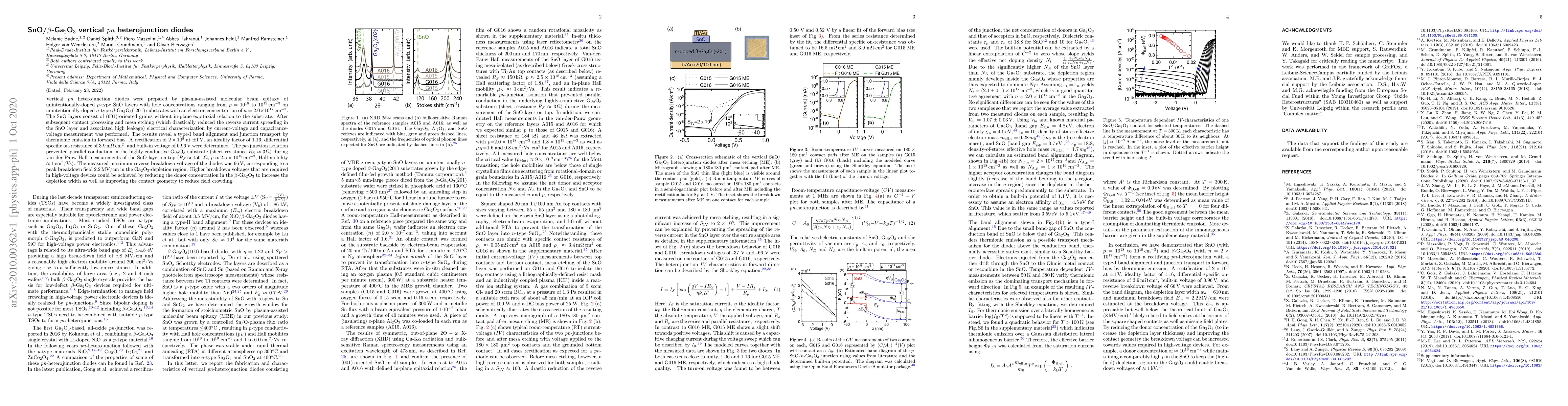
Vertical $pn$ heterojunction diodes were prepared by plasma-assisted molecular beam epitaxy of unintentionally-doped $p$-type SnO layers with hole concentrations ranging from $p=10^{18}$ to $10^{19}...

Thumbnail for Influence of Polymorphism on the Electronic Structure of Ga$_2$O$_3$
arXiv
Influence of Polymorphism on the Electronic Structure of Ga$_2$O$_3$

The search for new wide band gap materials is intensifying to satisfy the need for more advanced and energy efficient power electronic devices. Ga$_2$O$_3$ has emerged as an alternative to SiC and G...

Thumbnail for Towards smooth (010) beta-Ga2O3 films homoepitaxially grown by plasma
  assisted molecular beam epitaxy: The impact of substrate offcut and
  metal-to-oxygen flux ratio
arXiv
Towards smooth (010) beta-Ga2O3 films homoepitaxially grown by plasma assisted molecular beam epitaxy: The impact of substrate offcut and metal-to-oxygen flux ratio

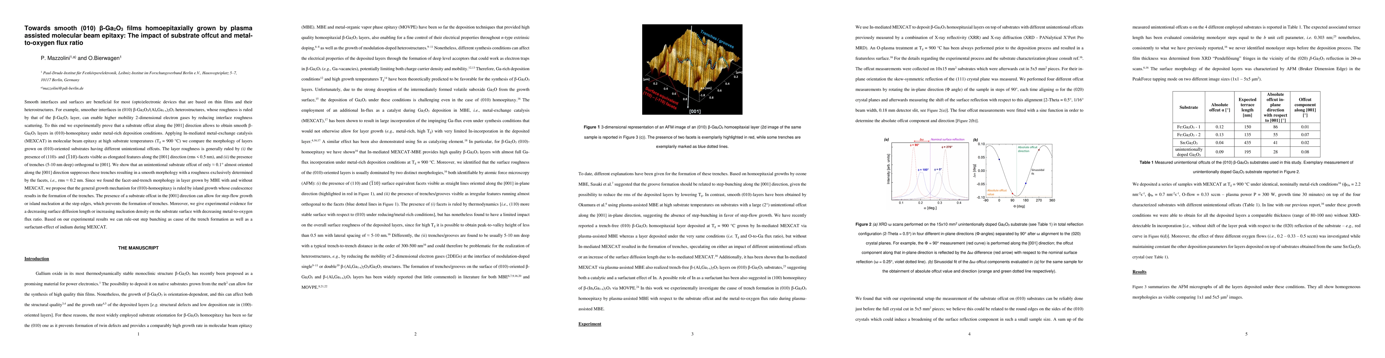
Smooth interfaces and surfaces are beneficial for most (opto)electronic devices based on thin films and their heterostructures. For example, smoother interfaces in (010) beta-Ga2O3/(AlxGa1-x)2O3 het...

Thumbnail for The two-dimensional electron gas of the In2O3 surface: Enhanced
  thermopower, electrical transport properties, and its reduction by adsorbates
  or compensating acceptor doping
arXiv
The two-dimensional electron gas of the In2O3 surface: Enhanced thermopower, electrical transport properties, and its reduction by adsorbates or compensating acceptor doping

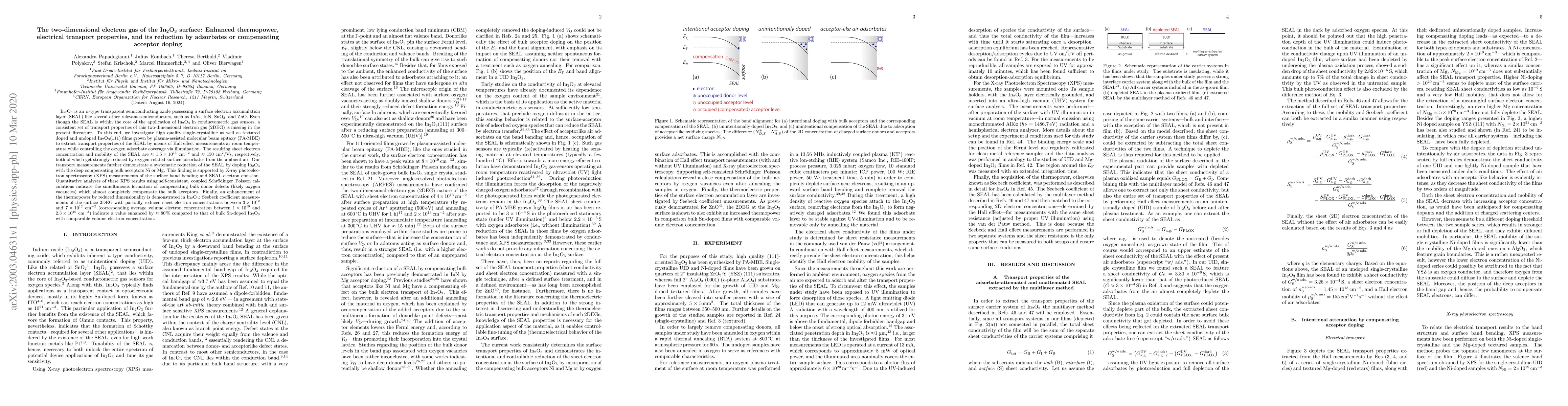
In2O3 is an n-type transparent semiconducting oxide possessing a surface electron accumulation layer (SEAL) like several other relevant semiconductors, such as InAs, InN, SnO2, and ZnO. Even though ...

Thumbnail for Structural, optical, and electrical properties of unintentionally doped
  NiO layers grown on MgO by plasma-assisted molecular beam epitaxy
arXiv
Structural, optical, and electrical properties of unintentionally doped NiO layers grown on MgO by plasma-assisted molecular beam epitaxy

NiO layers were grown on MgO(100), MgO(110), and MgO(111) substrates by plasma-assisted molecular beam epitaxy under Ni-flux limited growth conditions. Single crystalline growth with a cube-on-cube ...

Thumbnail for Plasma-assisted molecular beam epitaxy of NiO on GaN(00.1)
arXiv
Plasma-assisted molecular beam epitaxy of NiO on GaN(00.1)

The growth of NiO on GaN(00.1) substrates by plasma-assisted molecular beam epitaxy under oxygen rich conditions was investigated at growth temperatures between 100 $^{\circ}$C and 850 $^{\circ}$C. ...

Thumbnail for Kinetics, thermodynamics, and catalysis of the cation incorporation into
  GeO$_2$, SnO$_2$, and (Sn$_x$Ge$_{1-x}$)O$_2$ during suboxide molecular beam
  epitaxy
arXiv
Kinetics, thermodynamics, and catalysis of the cation incorporation into GeO$_2$, SnO$_2$, and (Sn$_x$Ge$_{1-x}$)O$_2$ during suboxide molecular beam epitaxy

Rutile GeO$_2$ is a promising ultra-wide bandgap semiconductor for future power electronic devices whose alloy with the wide bandgap semiconductor rutile-SnO$_2$ enables bandgap engineering and the fo...

Thumbnail for Enabling two-dimensional electron gas with high room-temperature
  electron mobility exceeding 100 cm$^2$/Vs at a perovskite oxide interface
arXiv
Enabling two-dimensional electron gas with high room-temperature electron mobility exceeding 100 cm$^2$/Vs at a perovskite oxide interface

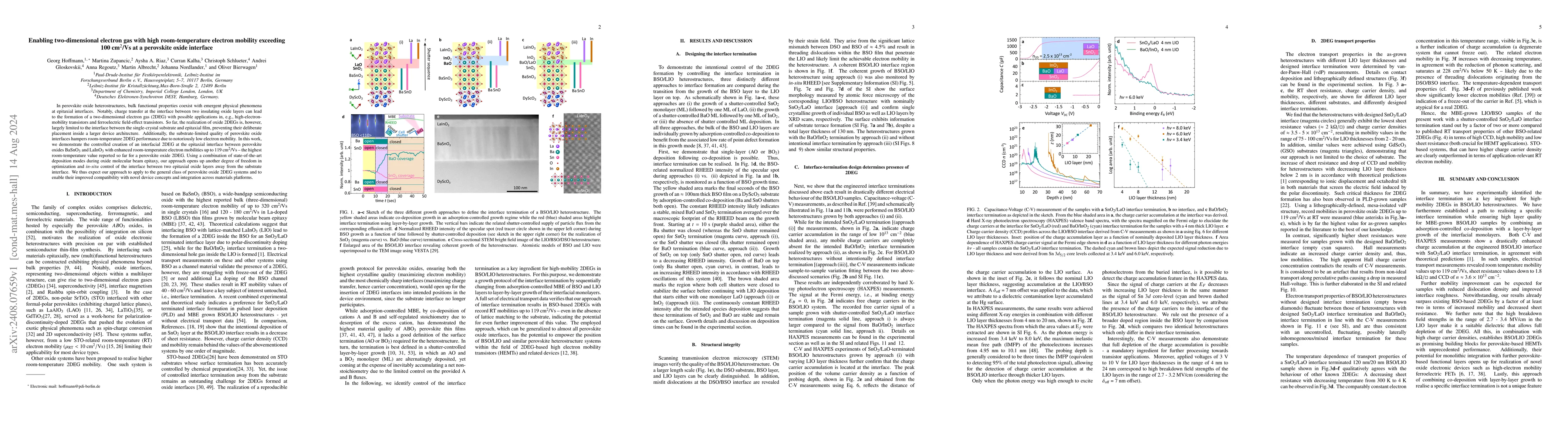
In perovskite oxide heterostructures, bulk functional properties coexist with emergent physical phenomena at epitaxial interfaces. Notably, charge transfer at the interface between two insulating oxid...

Thumbnail for Spectral tuning of hyperbolic shear polaritons in monoclinic gallium
  oxide via isotopic substitution
arXiv
Spectral tuning of hyperbolic shear polaritons in monoclinic gallium oxide via isotopic substitution

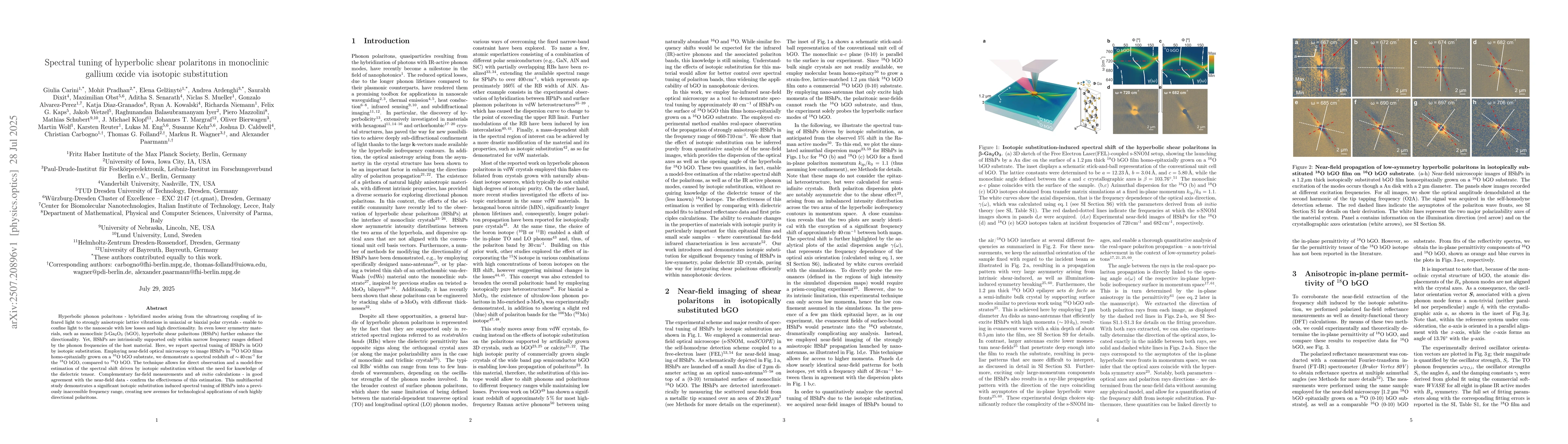
Hyperbolic phonon polaritons - hybridized modes arising from the ultrastrong coupling of infrared light to strongly anisotropic lattice vibrations in uniaxial or biaxial polar crystals - enable to con...

Thumbnail for $β$-Ga$_2$O$_3$(001) surface reconstructions from first principles
  and experiment
arXiv
$β$-Ga$_2$O$_3$(001) surface reconstructions from first principles and experiment

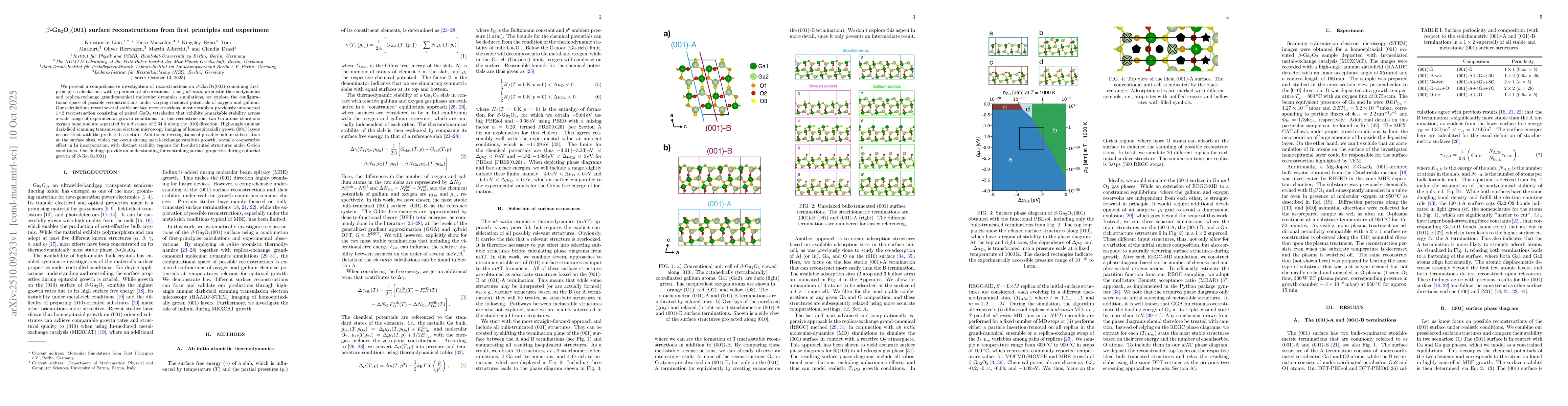
We present a comprehensive investigation of reconstructions on $\beta$-Ga$_2$O$_3$(001) combining first-principles calculations with experimental observations. Using {\it ab initio} atomistic thermody...

Thumbnail for Unravelling the oxygen influence in cubic bixbyite In$_2$O$_3$ on Raman
  active phonon modes by isotope studies
arXiv
Unravelling the oxygen influence in cubic bixbyite In$_2$O$_3$ on Raman active phonon modes by isotope studies

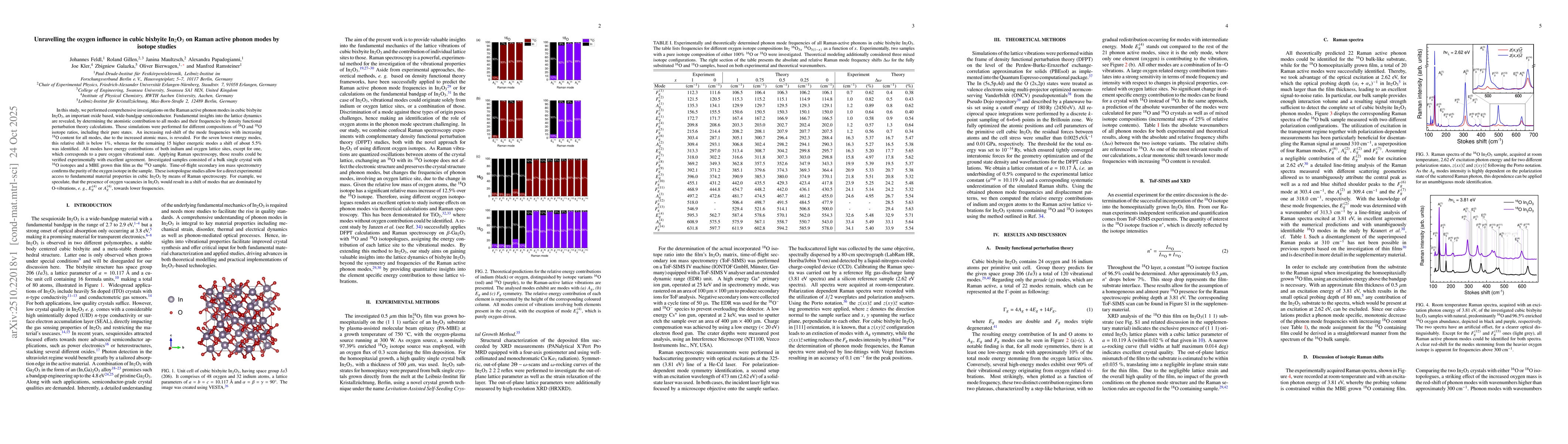
In this study, we performed comprehensive investigations on the Raman active phonon modes in cubic bixbyite In$_2$O$_3$, an important oxide based, wide-bandgap semiconductor. Fundamental insights into...

This website uses cookies to ensure you get the best experience. Learn more