Pawni Manchanda
1 papers on arXiv
Academic Profile
Statistics
arXiv Papers
1
Total Publications
1
Similar Authors
Papers on arXiv
Quantification of 2D Interfaces: Quality of heterostructures, and what is inside a nanobubble
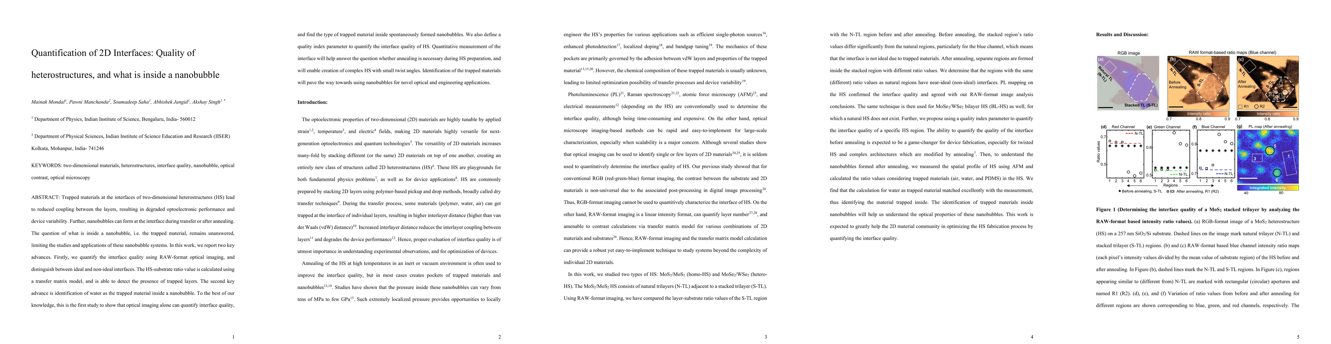
Trapped materials at the interfaces of two-dimensional heterostructures (HS) lead to reduced coupling between the layers, resulting in degraded optoelectronic performance and device variability. Fur...