ArxivLens
P
Researcher

Pedro Carlos Feijoo

11 papers on arXiv

11 arXiv Papers
33 Total Publications
Profile

Academic Profile

Name P. C. Feijoo
Total Papers 33
Scholar Profile View on Semantic Scholar
Metrics

Statistics

11 arXiv Papers
33 Total Publications
Publications

Papers on arXiv

Thumbnail for Anomalous thermal oxidation of gadolinium thin films deposited on
  silicon by high pressure sputtering
arXiv
Anomalous thermal oxidation of gadolinium thin films deposited on silicon by high pressure sputtering

Thin gadolinium metallic layers were deposited by high-pressure sputtering in pure Ar atmosphere. Subsequently, in situ thermal oxidation was performed at temperatures ranging from 150 to 750 $^\cir...

Thumbnail for Electrical characterization of gadolinium oxide deposited by high
  pressure sputtering with in situ plasma oxidation
arXiv
Electrical characterization of gadolinium oxide deposited by high pressure sputtering with in situ plasma oxidation

In this work, we characterized gadolinium oxide films deposited on silicon by high pressure sputtering with a two-step process: first, we sputtered metallic gadolinium in an argon atmosphere and the...

Thumbnail for Gadolinium scandate by high-pressure sputtering for future generations
  of high-k dielectrics
arXiv
Gadolinium scandate by high-pressure sputtering for future generations of high-k dielectrics

Gd-rich gadolinium scandate (Gd2-xScxO3) was deposited by high-pressure sputtering on (100) silicon by alternating the deposition of lower than 0.5 nm thick films of its binary components: Sc2O3 and...

Thumbnail for Scavenging effect on plasma oxidized Gd$_2$O$_3$ grown by high pressure
  sputtering on Si and InP substrates
arXiv
Scavenging effect on plasma oxidized Gd$_2$O$_3$ grown by high pressure sputtering on Si and InP substrates

In this work, we analyze the scavenging effect of titanium gates on metal insulator semiconductor capacitors composed of gadolinium oxide as dielectric material deposited on Si and InP substrates. T...

Thumbnail for High-k gadolinium scandate on Si obtained by high pressure sputtering
  from metal targets and in-situ plasma oxidation
arXiv
High-k gadolinium scandate on Si obtained by high pressure sputtering from metal targets and in-situ plasma oxidation

This article studies the physical and electrical behavior of Gd2-xScxO3 layers grown by high pressure sputtering from metallic Gd and Sc targets. The aim is to obtain a high permittivity dielectric ...

Thumbnail for High Pressure Sputtering For Kigh-k Dielectric Deposition. Is It Worth
  Trying?
arXiv
High Pressure Sputtering For Kigh-k Dielectric Deposition. Is It Worth Trying?

Our research group studies the deposition of high permittivity dielectrics by a non-standard method: high-pressure sputtering. The dielectrics studied here are gadolinium scandate deposited from die...

Thumbnail for Towards metal electrode interface scavenging of rare-earth scandates: A
  Sc2O3 and Gd2O3 study
arXiv
Towards metal electrode interface scavenging of rare-earth scandates: A Sc2O3 and Gd2O3 study

AmorphousGd2O3 and Sc2O3 thin films were deposited on Si by high-pressure sputtering (HPS). In order to reduce the uncontrolled interfacial SiOx growth, firstly a metallic film of Gd or Sc was sputt...

Thumbnail for Optimization of gadolinium oxide growth deposited on Si by high pressure
  sputtering
arXiv
Optimization of gadolinium oxide growth deposited on Si by high pressure sputtering

High k gadolinium oxide thin layers were deposited on silicon by high-pressure sputtering (HPS). In order to optimize the properties for microelectronic applications, different deposition conditions...

Thumbnail for Optimization of scandium oxide growth by high pressure sputtering on
  silicon
arXiv
Optimization of scandium oxide growth by high pressure sputtering on silicon

This work demonstrates the viability of scandium oxide deposition on silicon by means of high pressure sputtering. Deposition pressure and radio frequency power are varied for optimization of the pr...

Thumbnail for Unveiling the impact of the bias-dependent charge neutrality point on
  graphene-based multi-transistor applications
arXiv
Unveiling the impact of the bias-dependent charge neutrality point on graphene-based multi-transistor applications

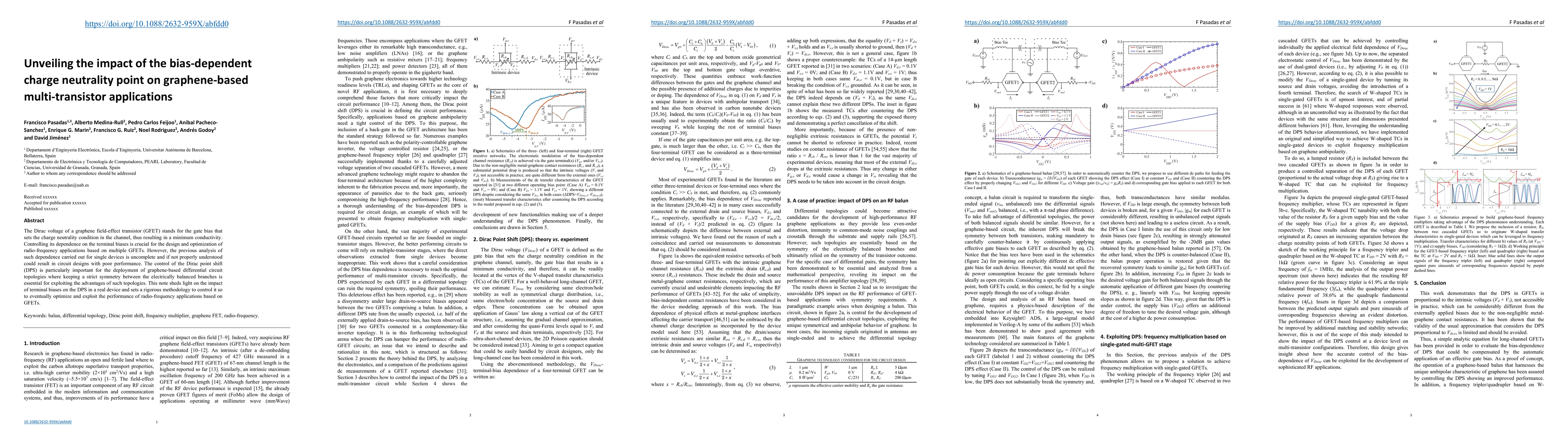
The Dirac voltage of a graphene field-effect transistor (GFET) stands for the gate bias that sets the charge neutrality condition in the channel, thus resulting in a minimum conductivity. Controllin...

Thumbnail for Does carrier velocity saturation help to enhance fmax in graphene
  field-effect transistors?
arXiv
Does carrier velocity saturation help to enhance fmax in graphene field-effect transistors?

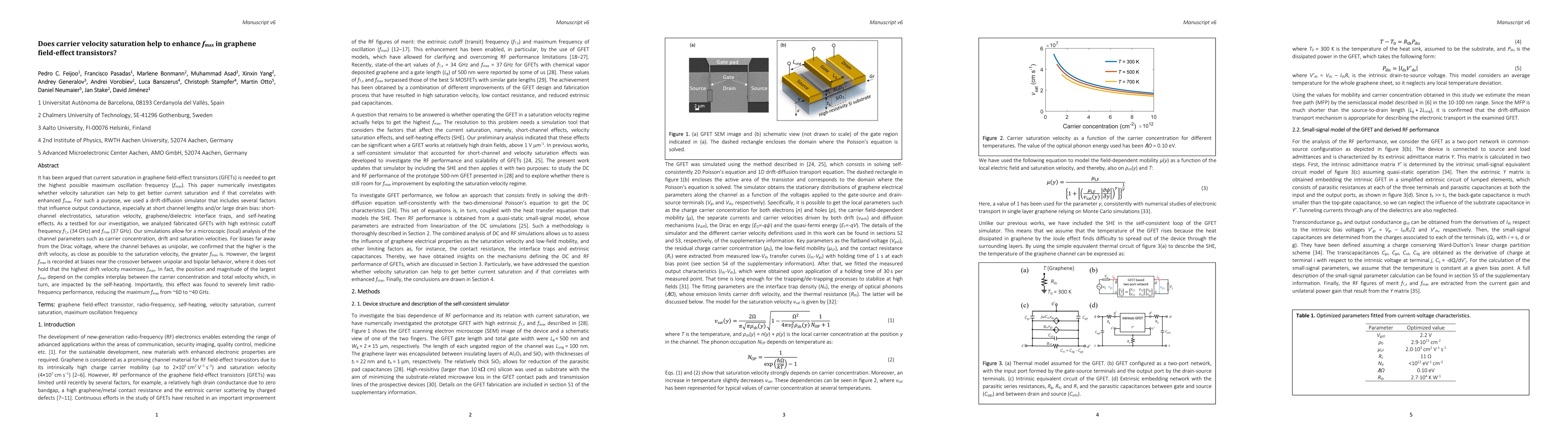
It has been argued that current saturation in graphene field-effect transistors (GFETs) is needed to get the highest possible maximum oscillation frequency (fmax). This paper numerically investigate...

This website uses cookies to ensure you get the best experience. Learn more