Academic Profile
Statistics
Similar Authors
Papers on arXiv
Dielectric optical resonators traditionally rely on materials with the combination of high refractive indices and low optical losses. Such materials are scarce for operation in visible spectrum and ...
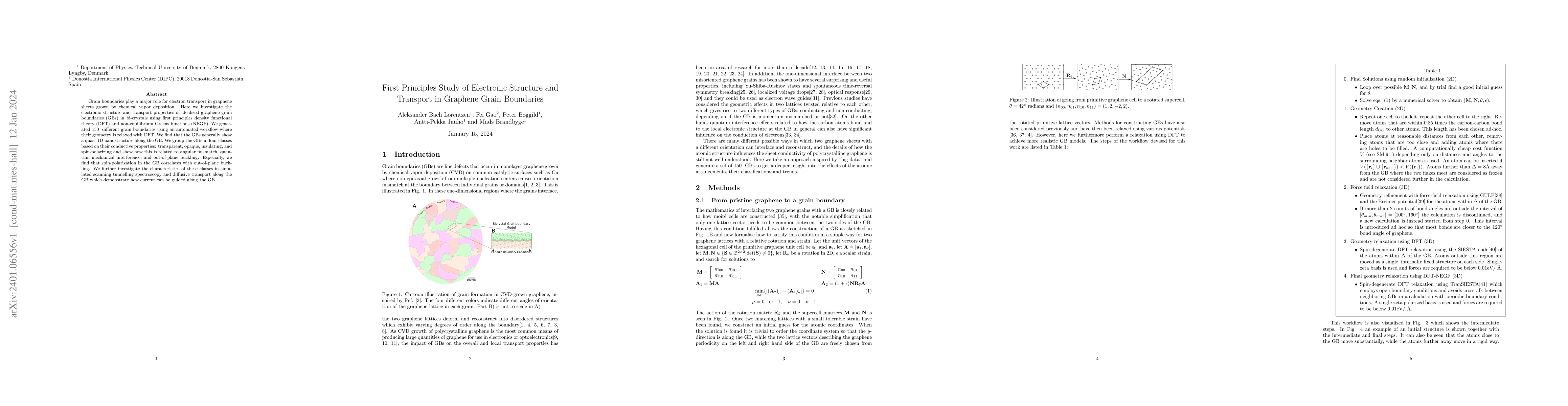
Grain boundaries play a major role for electron transport in graphene sheets grown by chemical vapor deposition. Here we investigate the electronic structure and transport properties of idealized gr...
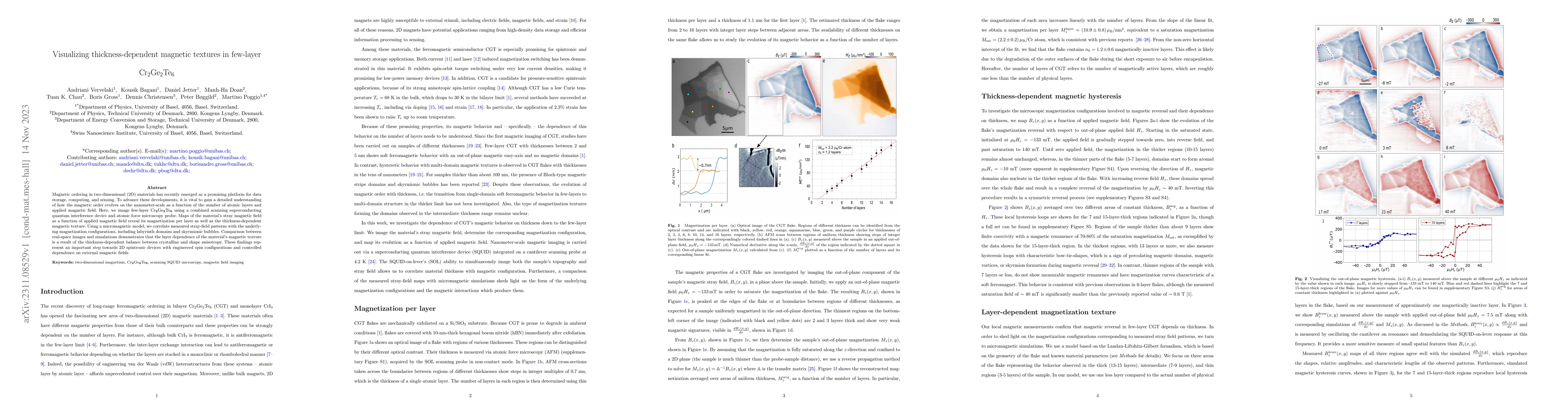
Magnetic ordering in two-dimensional (2D) materials has recently emerged as a promising platform for data storage, computing, and sensing. To advance these developments, it is vital to gain a detail...
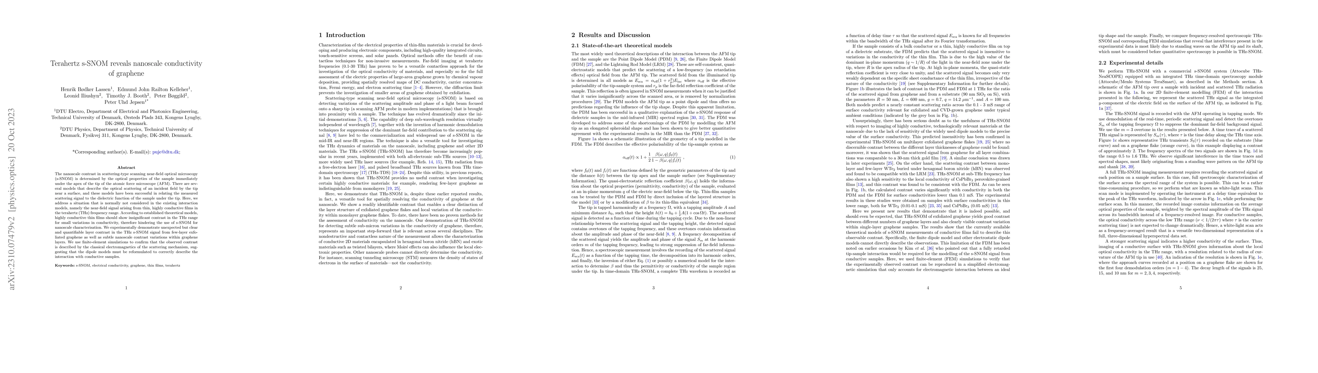
The nanoscale contrast in scattering-type scanning near-field optical microscopy (s-SNOM) is determined by the optical properties of the sample immediately under the apex of the tip of the atomic fo...
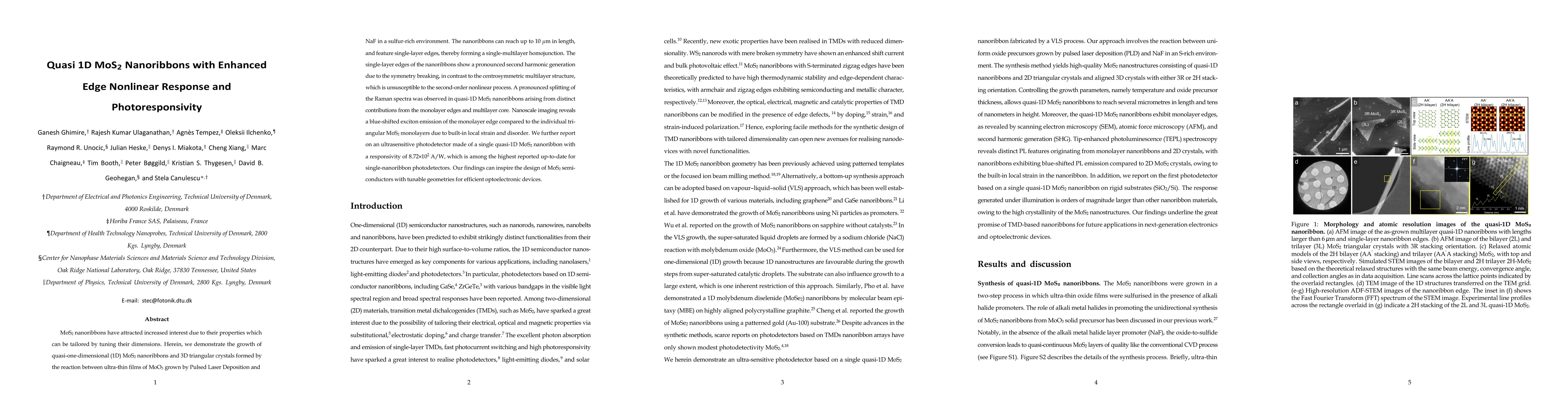
Molybdenum disulfide (MoS$_2$) nanoribbons have attracted increased interest due to their properties which can be tailored by tuning their dimensions. Herein, we demonstrate the growth of highly cry...
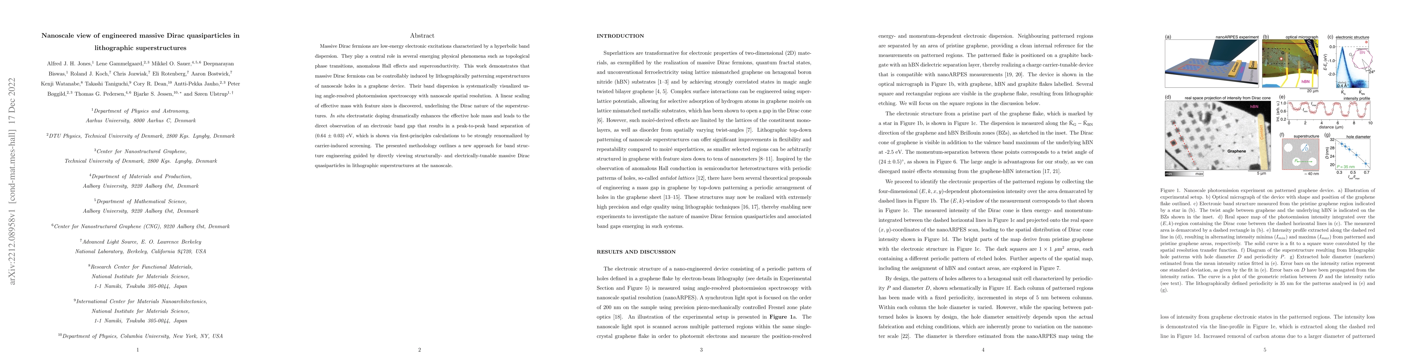
Massive Dirac fermions are low-energy electronic excitations characterized by a hyperbolic band dispersion. They play a central role in several emerging physical phenomena such as topological phase ...
Moir\'e superlattices in twisted two-dimensional materials have generated tremendous excitement as a platform for achieving quantum properties on demand. However, the moir\'e pattern is highly sensi...
Strong Fermi level pinning (FLP) - often attributed to metal-induced gap states at the interfacial contacts - severely reduces the tunability of the Schottky barrier height of the junction and limit...
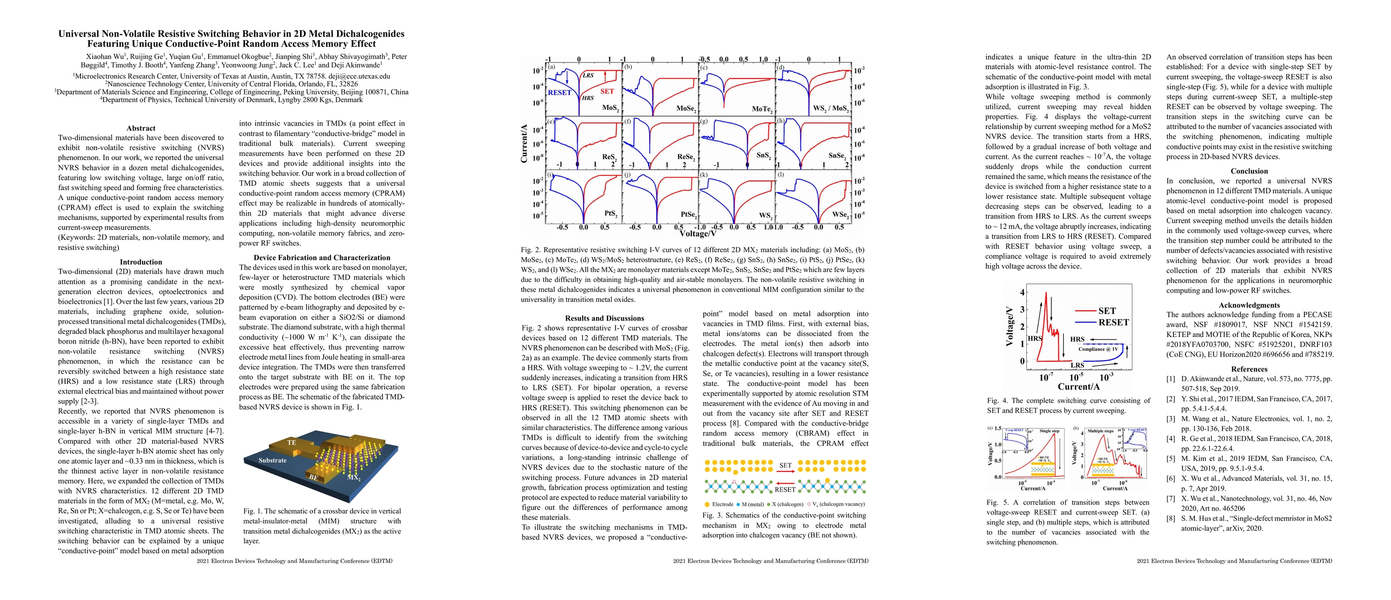
Two-dimensional materials have been discovered to exhibit non-volatile resistive switching (NVRS) phenomenon. In our work, we reported the universal NVRS behavior in a dozen metal dichalcogenides, f...
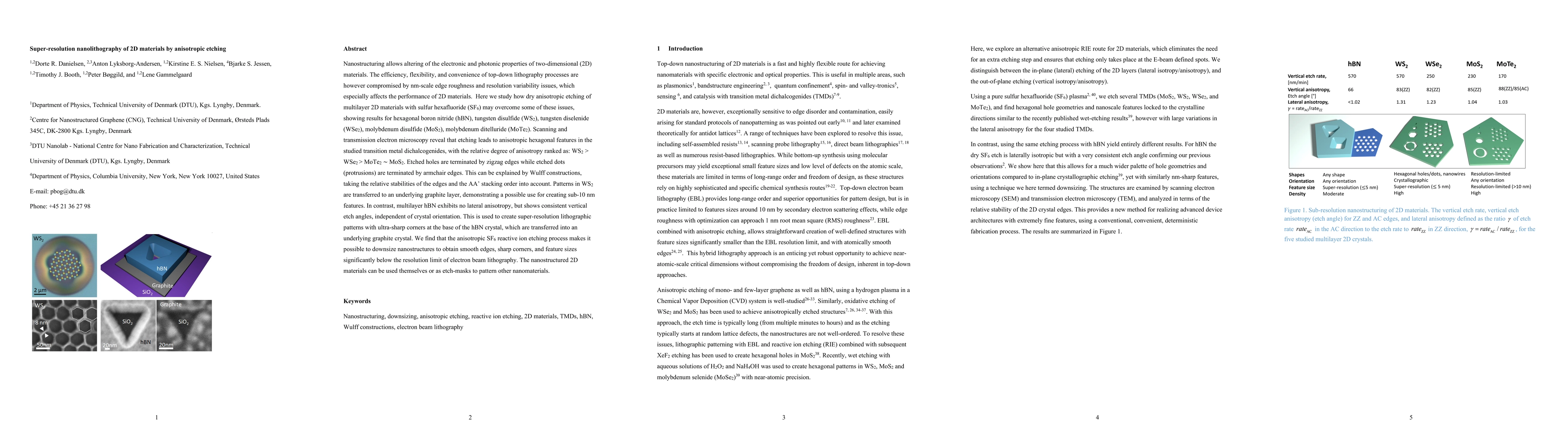
Nanostructuring allows altering of the electronic and photonic properties of two-dimensional (2D) materials. The efficiency, flexibility, and convenience of top-down lithography processes are howeve...
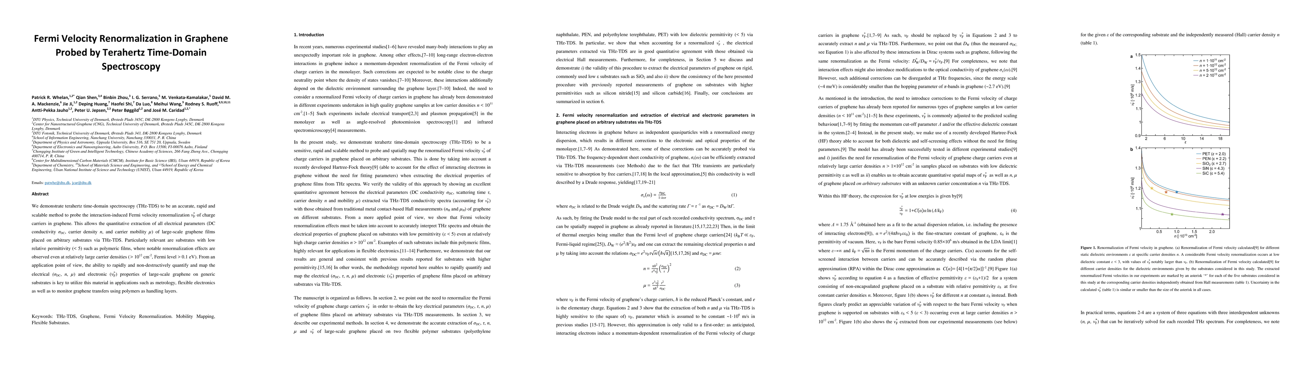
We demonstrate terahertz time-domain spectroscopy (THz-TDS) to be an accurate, rapid and scalable method to probe the interaction-induced Fermi velocity renormalization {\nu}F^* of charge carriers i...
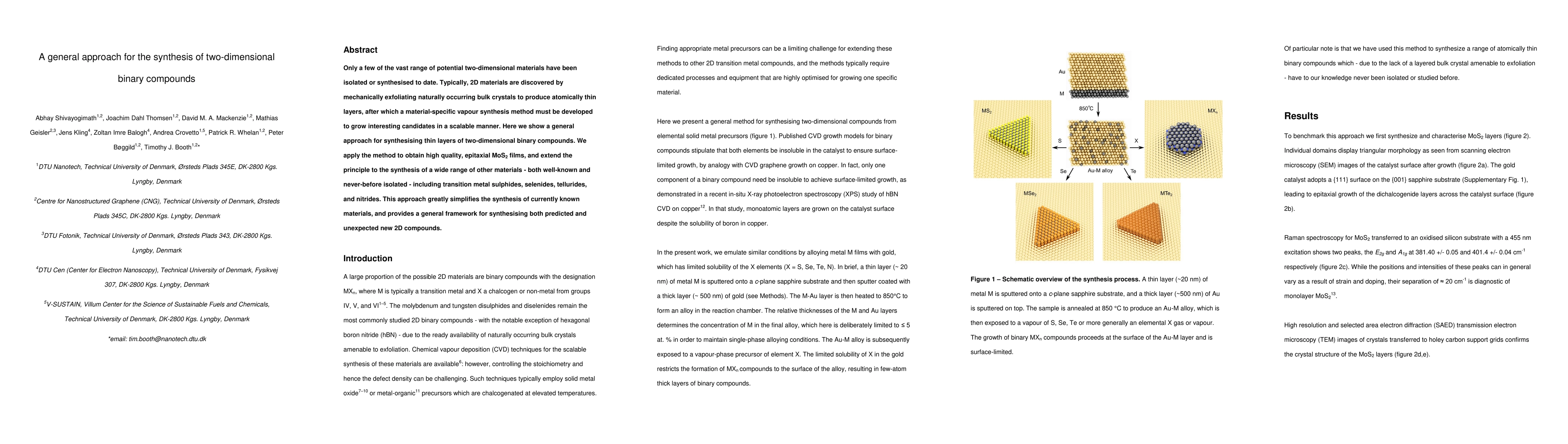
Only a few of the vast range of potential two-dimensional materials have been isolated or synthesised to date. Typically, 2D materials are discovered by mechanically exfoliating naturally occurring ...

2D materials research has reached significant scientific milestones, accompanied by a rapidly growing industrial sector in the two decades since the field's inception. Such rapid progress requires pus...
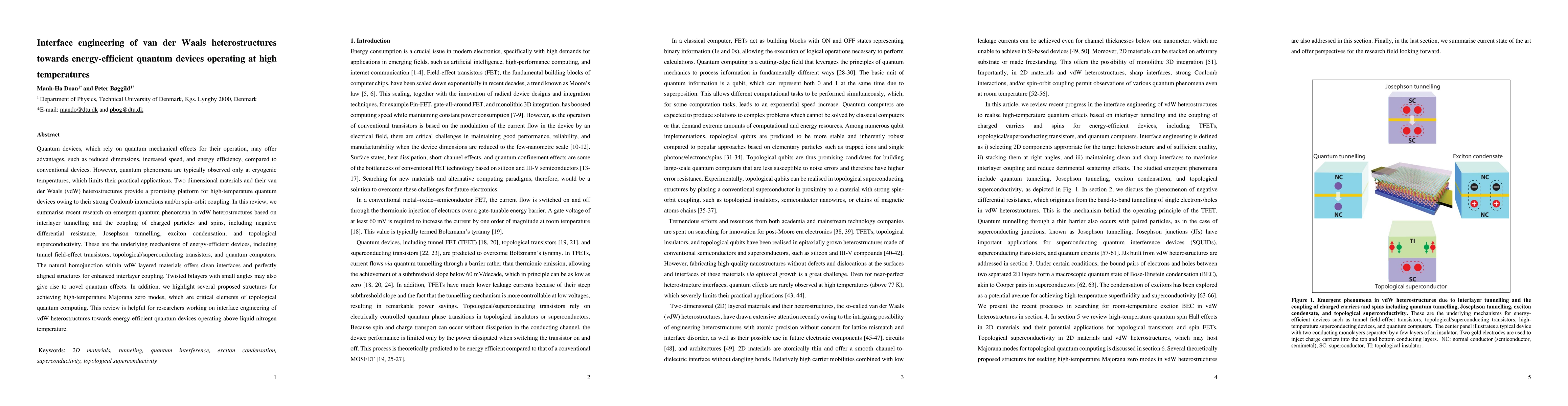
Quantum devices, which rely on quantum mechanical effects for their operation, may offer advantages, such as reduced dimensions, increased speed, and energy efficiency, compared to conventional device...
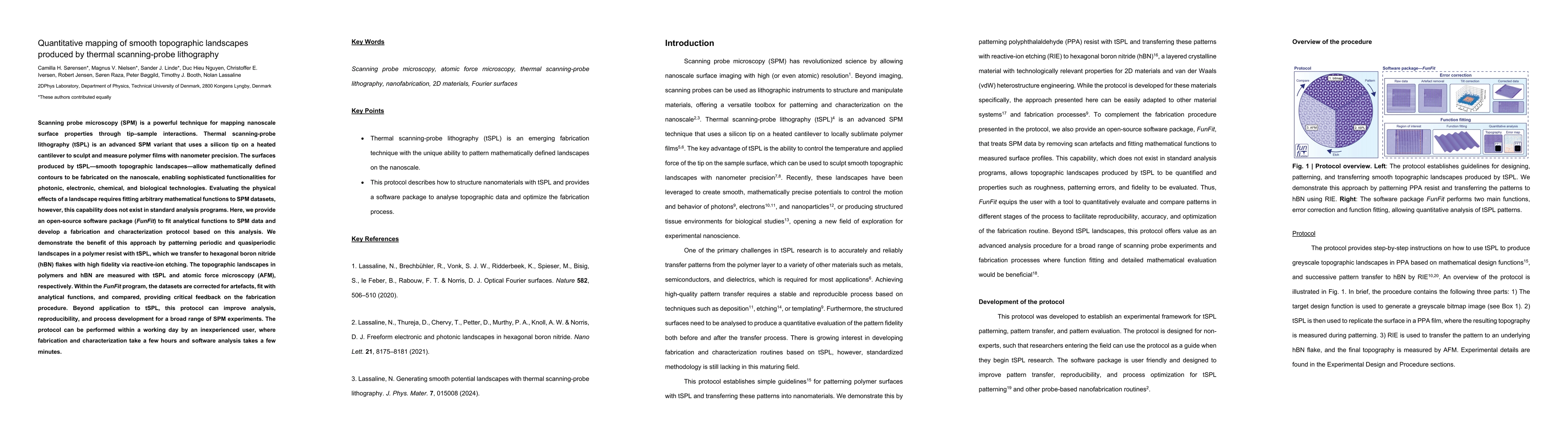
Scanning probe microscopy (SPM) is a powerful technique for mapping nanoscale surface properties through tip-sample interactions. Thermal scanning-probe lithography (tSPL) is an advanced SPM variant t...
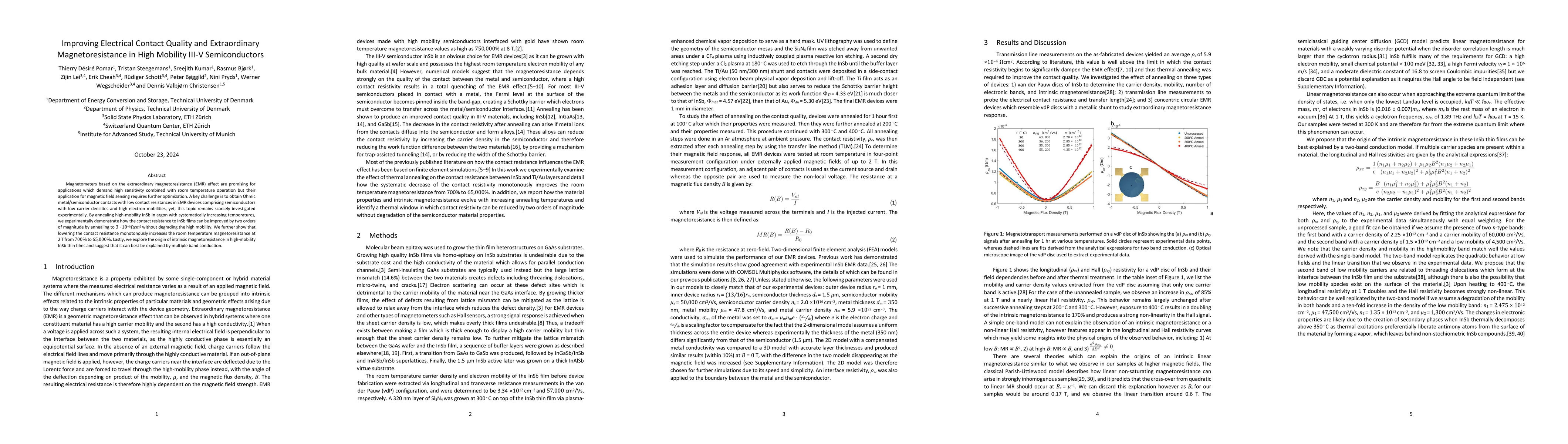
Magnetometers based on the extraordinary magnetoresistance (EMR) effect are promising for applications which demand high sensitivity combined with room temperature operation but their application for ...
Over the past two decades, 2D materials have rapidly evolved into a diverse and expanding family of material platforms. Many members of this materials class have demonstrated their potential to delive...
Two-dimensional (2D) materials such as graphene and hexagonal boron nitride (hBN) provide a versatile platform for quantum electronics. Experiments generally require encapsulating graphene within hBN ...
Thin films of high-refractive-index excitonic materials enable self-coupling by simultaneously supporting intrinsic excitonic transitions and optical resonances. These optical resonances take the form...