Quentin Ramasse

5 papers on arXiv

Academic Profile

Name: Quentin M Ramasse
Total Papers: 22

Statistics

arXiv Papers 5
Total Publications 22

Papers on arXiv

Thumbnail for Plasmons in MoS2 Studied via Experimental and Theoretical Correlation of
  Energy Loss Spectra

Plasmons in MoS2 Studied via Experimental and Theoretical Correlation of Energy Loss Spectra

Two dimensional materials offer a path forward for smaller and more efficient devices. Their optical and electronic properties give way to beat the limits set in place by Moore's Law. Plasmon are th...

Thumbnail for Bandgap in orthorhombic thin lead halide perovskite (CsPbBr3) nanosheets
  measured from STEM-EELS

Bandgap in orthorhombic thin lead halide perovskite (CsPbBr3) nanosheets measured from STEM-EELS

Inorganic lead halide perovskites are promising candidates for optoelectronic applications, due to their bandgap tunability, high photoluminescence quantum yield, and narrow emission line widths. In...

Thumbnail for Enhanced spin-orbit coupling in a heavy metal via molecular coupling

Enhanced spin-orbit coupling in a heavy metal via molecular coupling

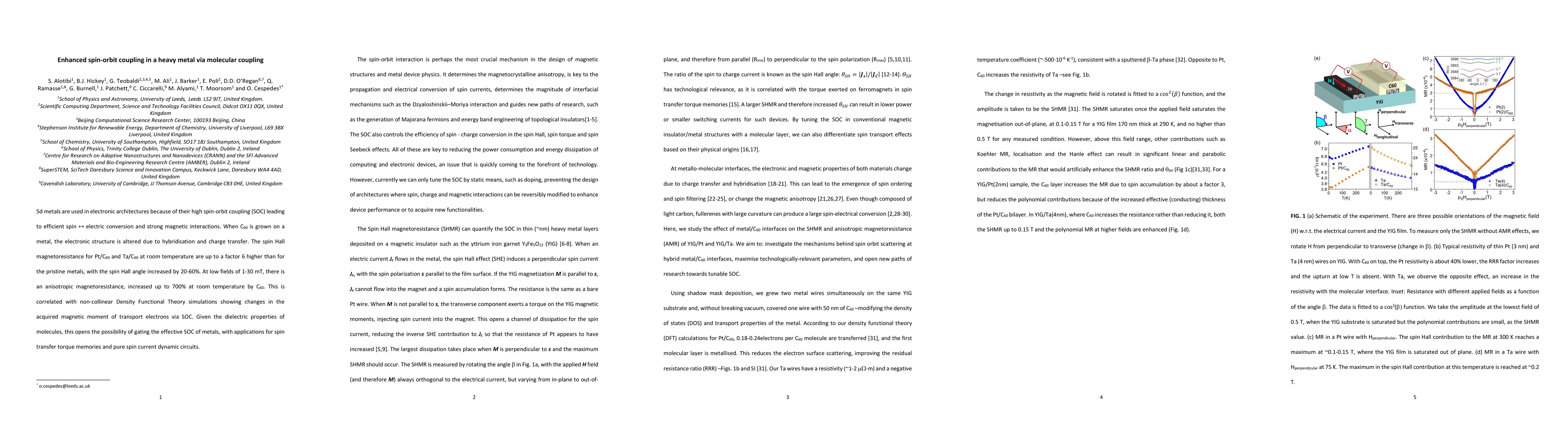
Heavy metals are key to spintronics because of their high spin-orbit coupling (SOC) leading to efficient spin conversion and strong magnetic interactions. When C60 is deposited on Pt, the molecular ...

Thumbnail for Imaging localized plasmon resonances in vacancy doped Cu3-xP
  semiconductor nanocrystals with STEM-EELS

Imaging localized plasmon resonances in vacancy doped Cu3-xP semiconductor nanocrystals with STEM-EELS

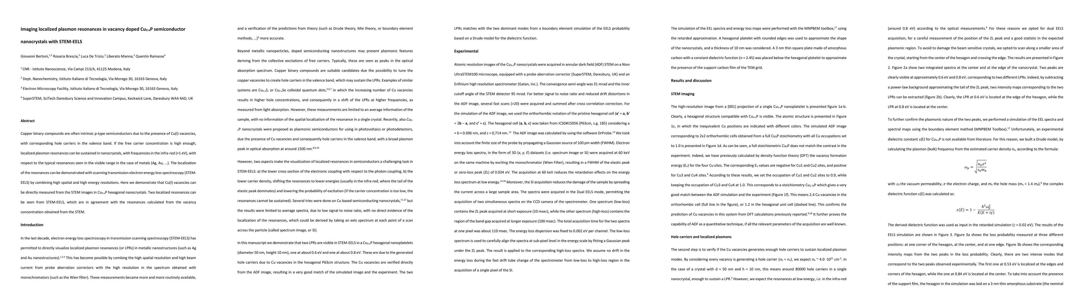
Copper binary compounds are often intrinsic p-type semiconductors due to the presence of Cu(I) vacancies, with corresponding hole carriers in the valence band. If the free carrier concentration is h...

Thumbnail for Control of 2D plasmons in the topological insulator Bi2Se3 with highly
  crystalline C60 overlayers

Control of 2D plasmons in the topological insulator Bi2Se3 with highly crystalline C60 overlayers

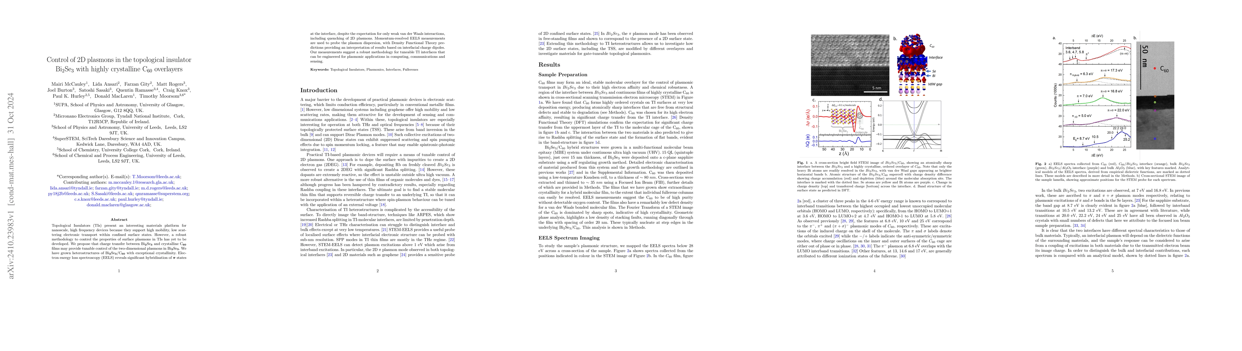
Topological Insulators (TIs) present an interesting materials platform for nanoscale, high frequency devices because they support high mobility, low scattering electronic transport within confined sur...

This website uses cookies to ensure you get the best experience. Learn more