Academic Profile
Statistics
Similar Authors
Papers on arXiv
In this radiation tolerance study, Low Gain Avalanche Detectors (LGADs) with a carbon-enriched broad and shallow multiplication layer were examined in comparison to identical non-carbonated LGADs. M...
We demonstrate synthesis of BaZr(S,Se)3 chalcogenide perovskite alloys by selenization of BaZrS3 thin films. The anion-exchange process produces films with tunable composition and band gap without c...
We report a comparative study of temperature-dependent photoluminescence and structural dynamics of two perovskite semiconductors, the chalcogenide BaZrS$_3$ (BZS) and the halide CsPbBr$_3$ (CPB). T...
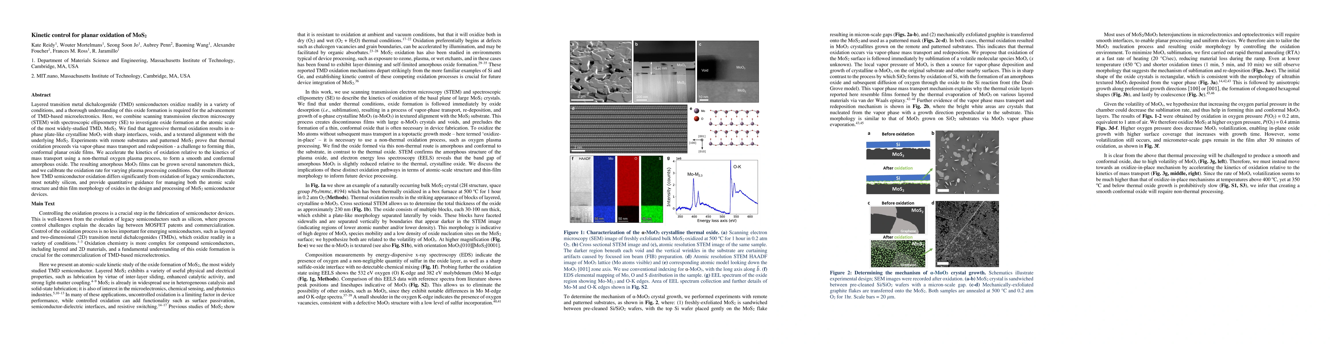
Layered transition metal dichalcogenide (TMD) semiconductors oxidize readily in a variety of conditions, and a thorough understanding of this oxide formation is required for the advancement of TMD-b...
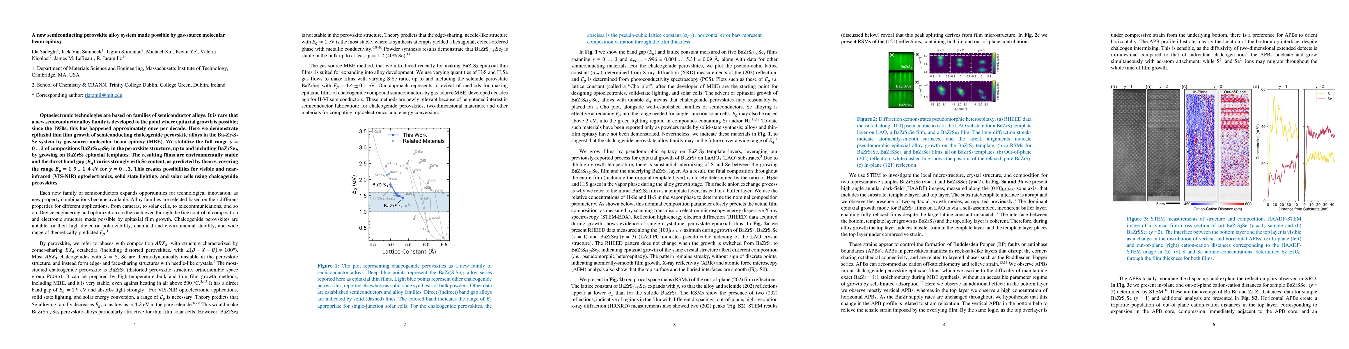
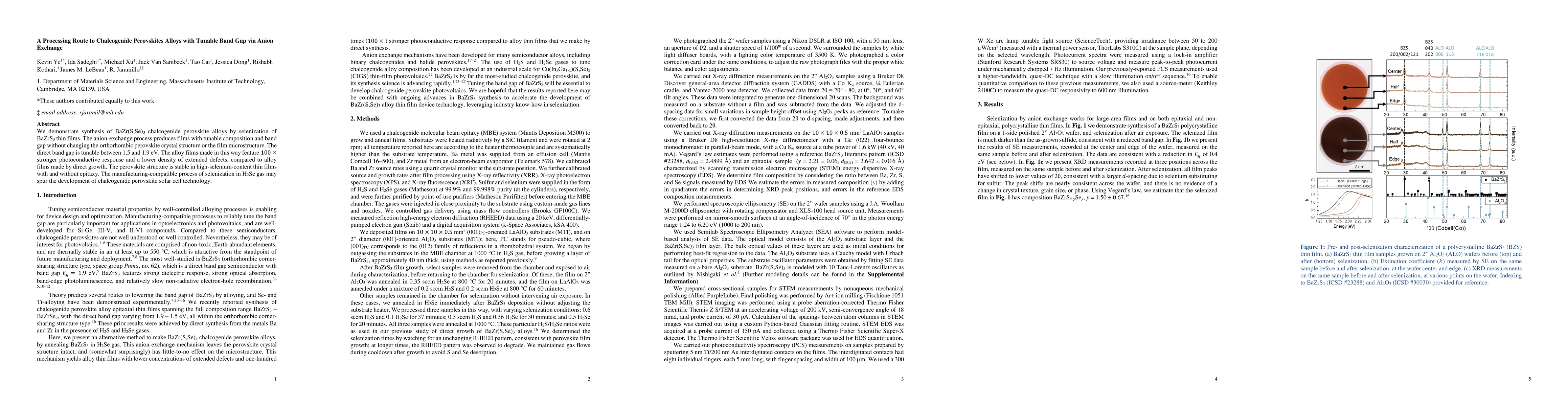
Optoelectronic technologies are based on families of semiconductor alloys. It is rare that a new semiconductor alloy family is developed to the point where epitaxial growth is possible; since the 19...
Many semiconductors feature defects with charge state transition levels that can switch due to structure changes following defect ionization: we call this defect-level switching (DLS). For example, ...
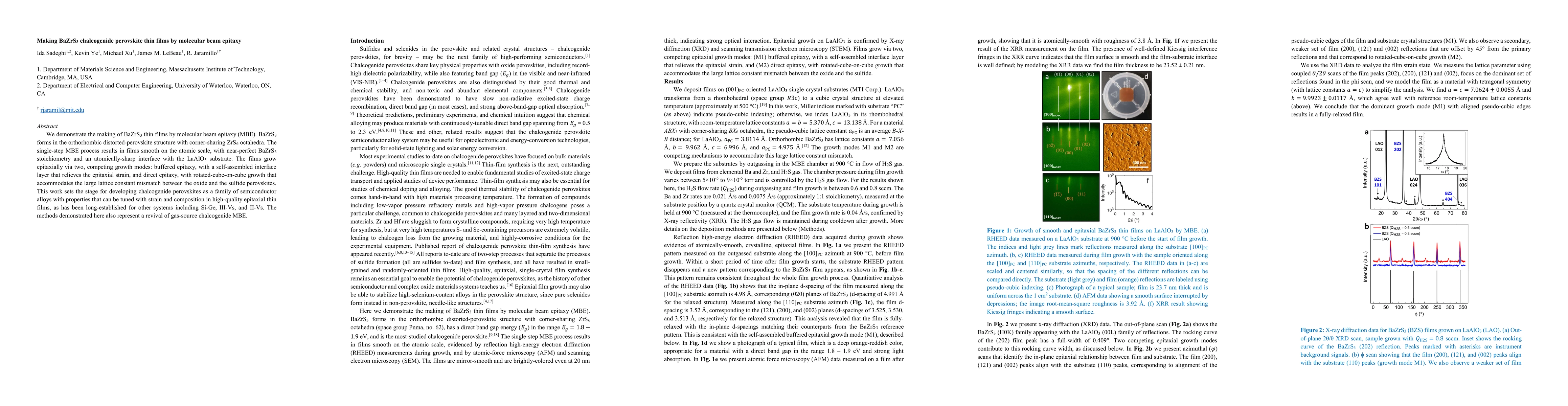
We demonstrate the making of BaZrS3 thin films by molecular beam epitaxy (MBE). BaZrS3 forms in the orthorhombic distorted-perovskite structure with corner-sharing ZrS6 octahedra. The single-step MB...
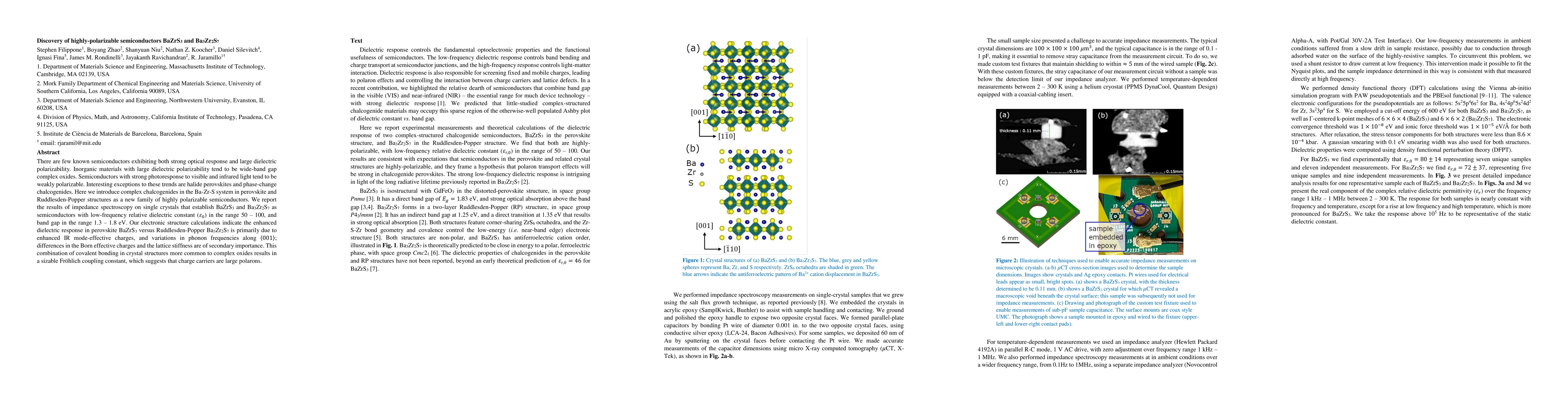
There are few known semiconductors exhibiting both strong optical response and large dielectric polarizability. Inorganic materials with large dielectric polarizability tend to be wide-band gap comp...
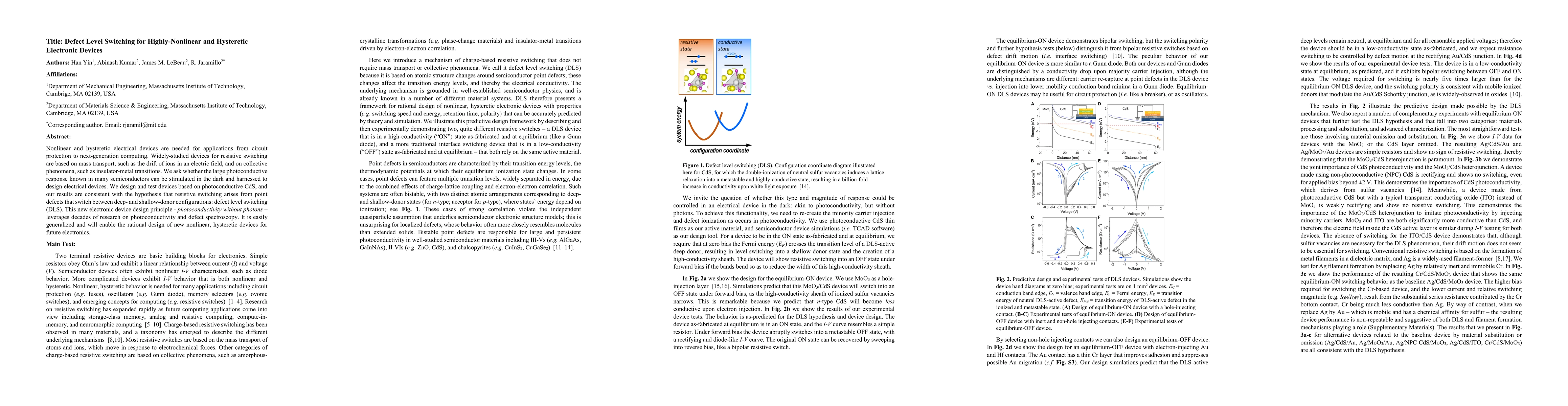
Nonlinear and hysteretic electrical devices are needed for applications from circuit protection to next-generation computing. Widely-studied devices for resistive switching are based on mass transpo...
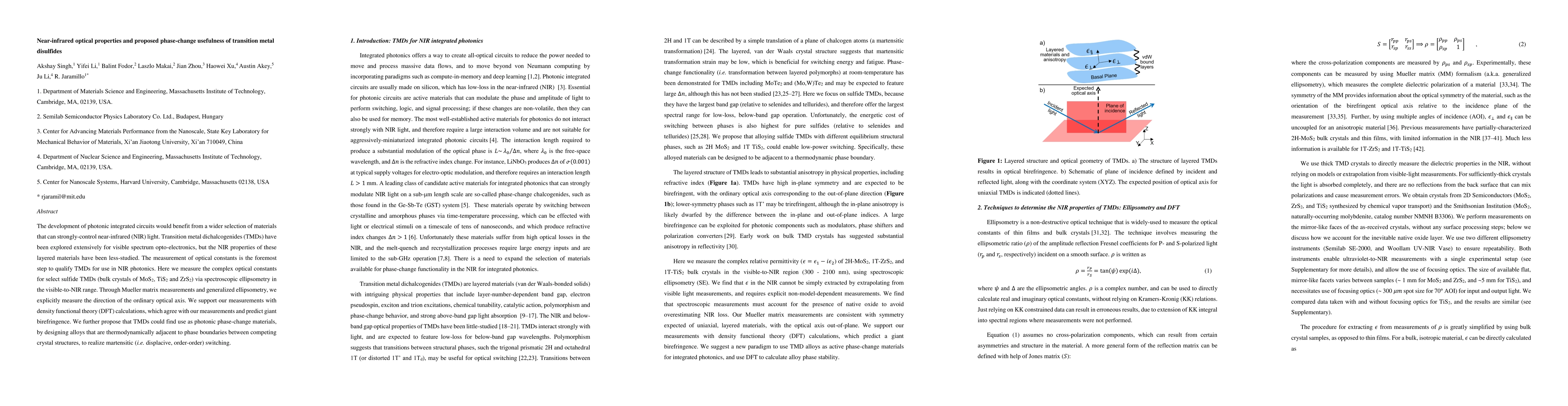
The development of photonic integrated circuits would benefit from a wider selection of materials that can strongly-control near-infrared (NIR) light. Transition metal dichalcogenides (TMDs) have be...
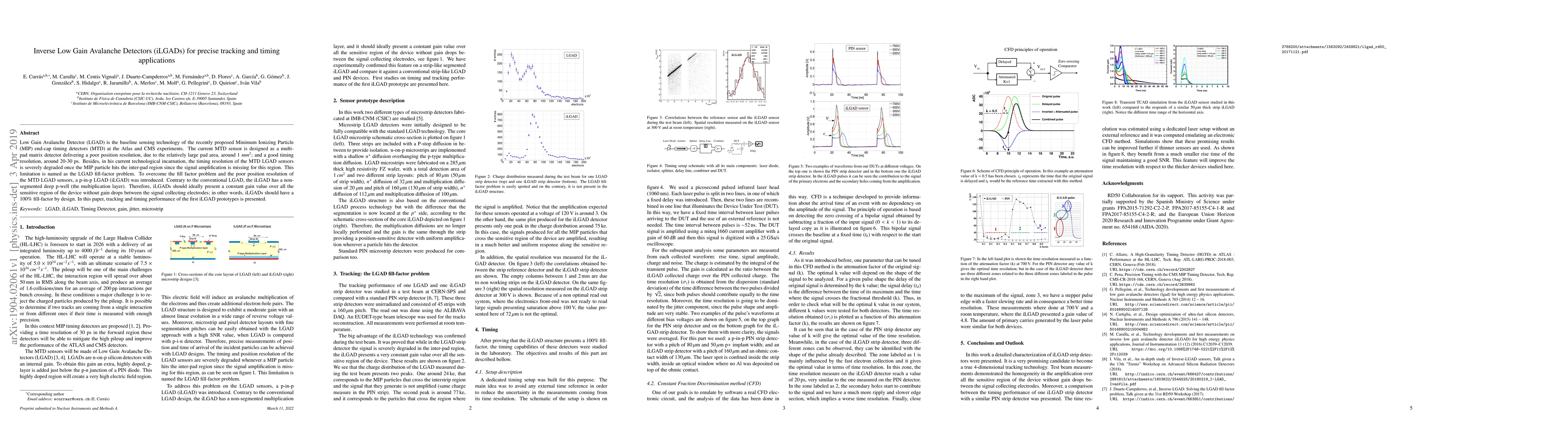
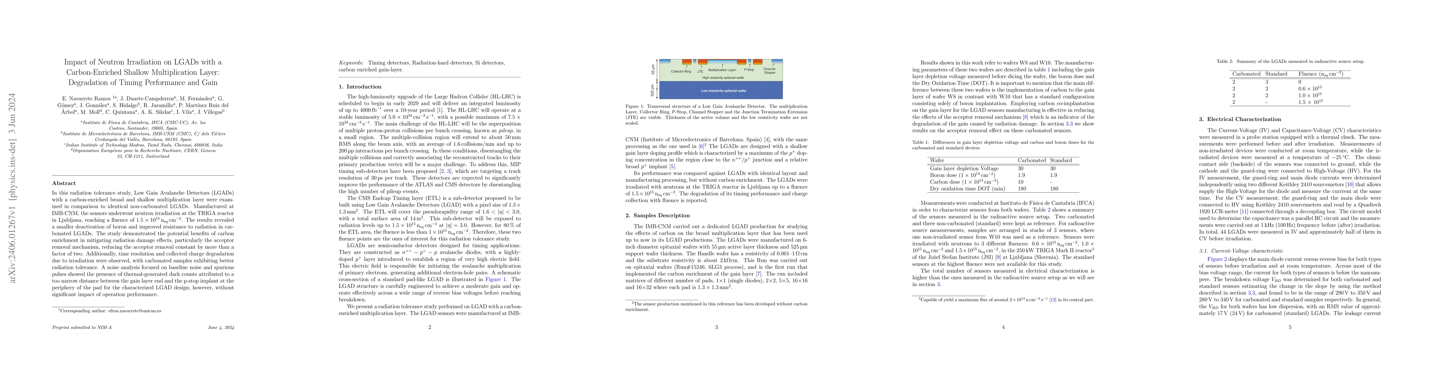
Low Gain Avalanche Detector (LGAD) is the baseline sensing technology of the recently proposed Minimum Ionizing Particle (MIP) end-cap timing detectors (MTD) at the Atlas and CMS experiments. The cu...
In this paper we review the physics opportunities at linear $e^+e^-$ colliders with a special focus on high centre-of-mass energies and beam polarisation, take a fresh look at the various accelerator ...
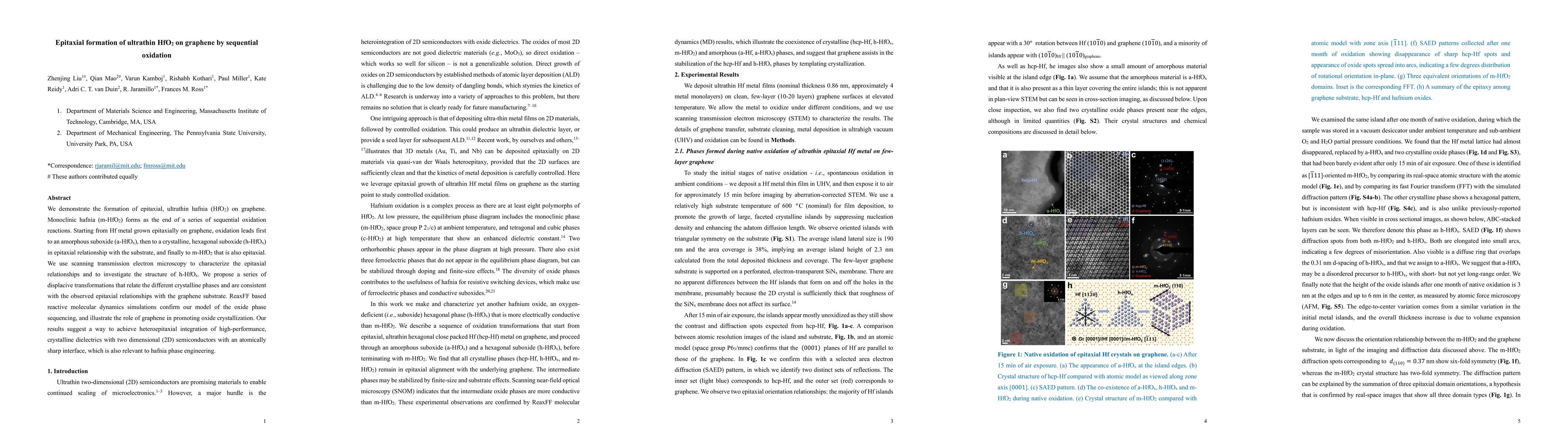
We demonstrate the formation of epitaxial, ultrathin hafnia (HfO2) on graphene. Monoclinic hafnia (m-HfO2) forms as the end of a series of sequential oxidation reactions. Starting from Hf metal grown ...
In this paper we outline a proposal for a Linear Collider Facility as the next flagship project for CERN. It offers the opportunity for a timely, cost-effective and staged construction of a new collid...
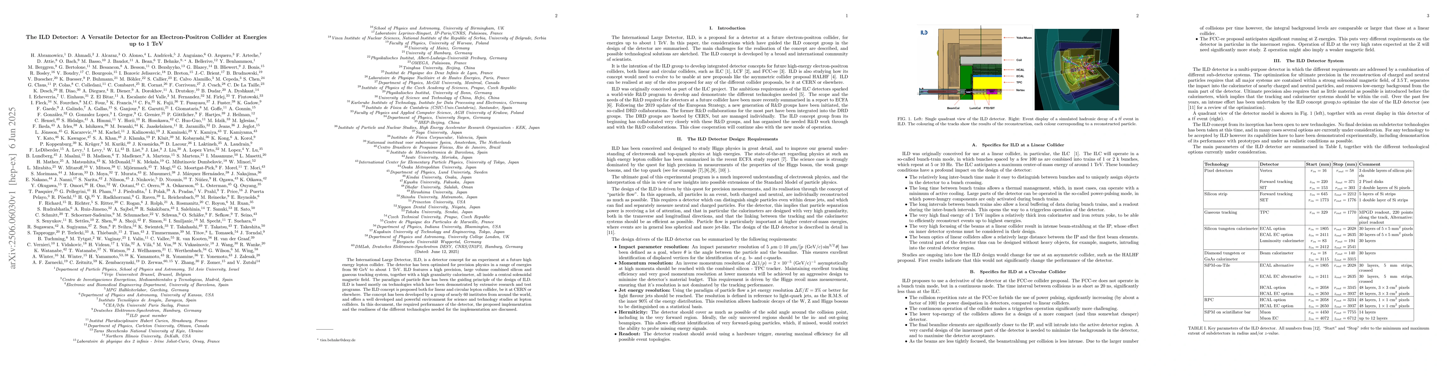
The International Large Detector, ILD, is a detector concept for an experiment at a future high energy lepton collider. The detector has been optimised for precision physics in a range of energies fro...
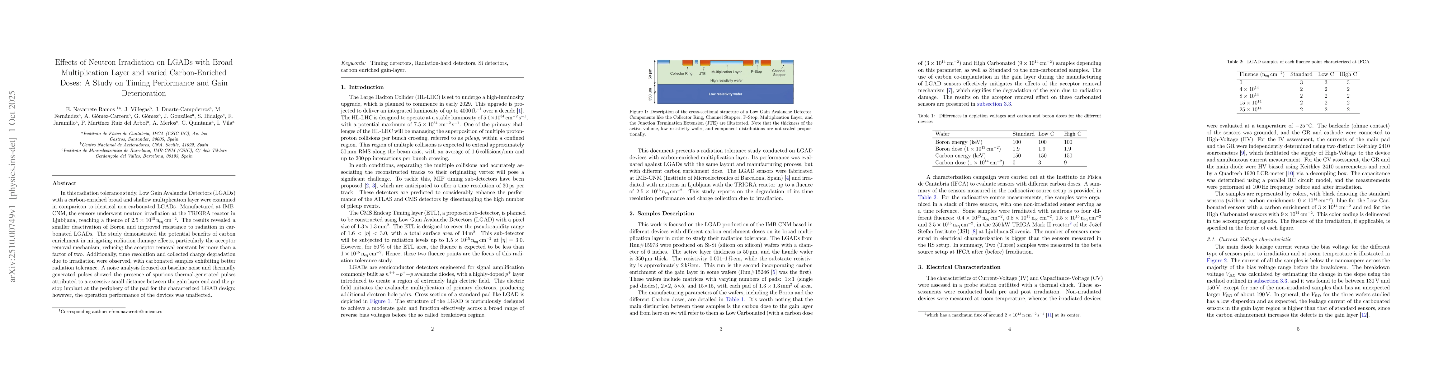
In this radiation tolerance study, Low Gain Avalanche Detectors (LGADs) with a carbon-enriched broad and shallow multiplication layer were examined in comparison to identical non-carbonated LGADs. Man...