Academic Profile
Statistics
Similar Authors
Papers on arXiv
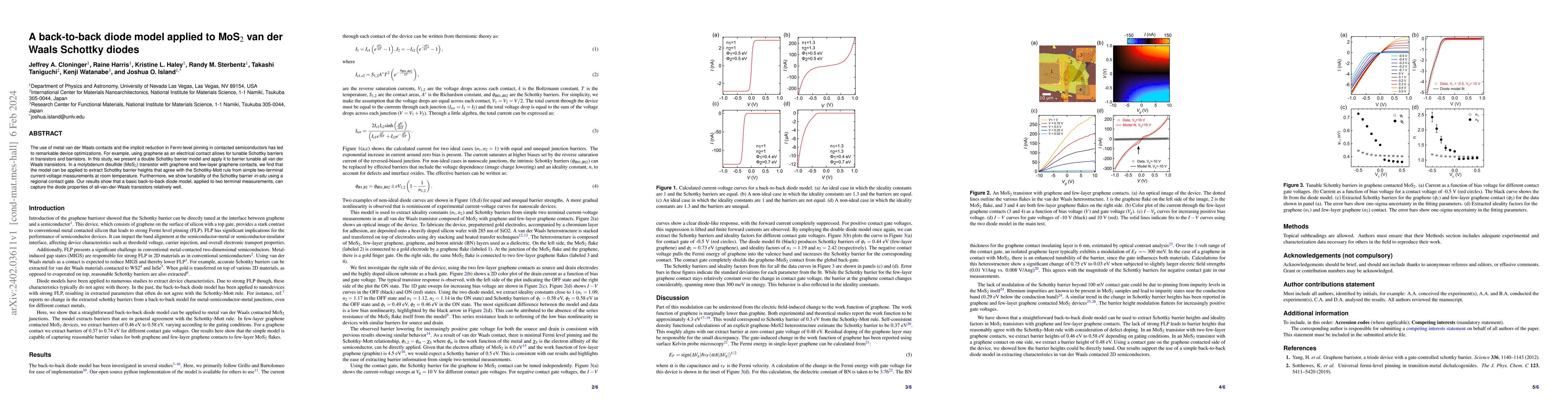
The use of metal van der Waals contacts and the implicit reduction in Fermi-level pinning in contacted semiconductors has led to remarkable device optimizations. For example, using graphene as an el...
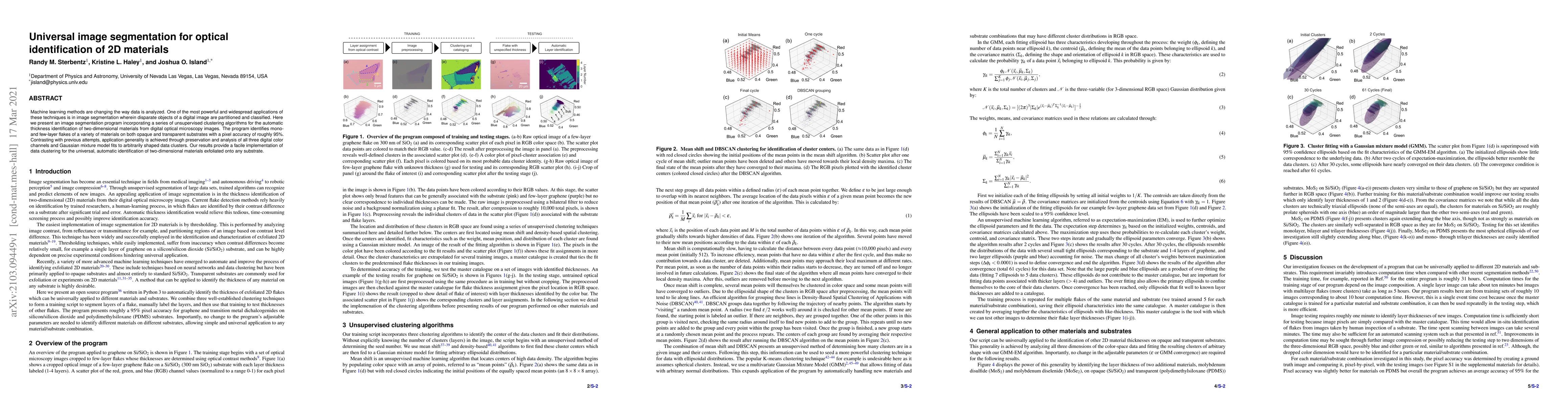
Machine learning methods are changing the way data is analyzed. One of the most powerful and widespread applications of these techniques is in image segmentation wherein disparate objects of a digit...
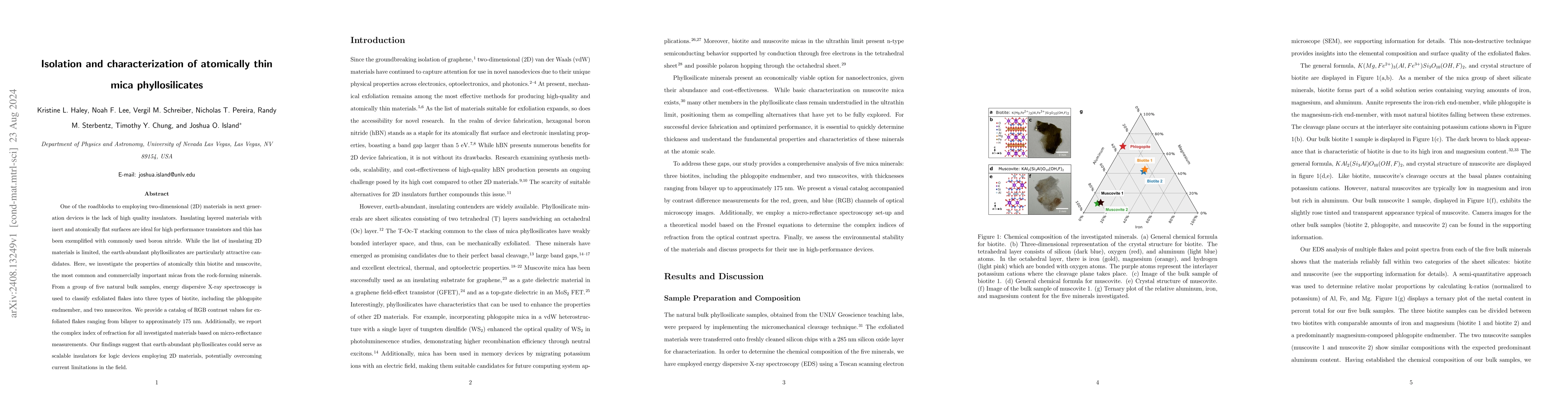
One of the roadblocks to employing two-dimensional (2D) materials in next generation devices is the lack of high quality insulators. Insulating layered materials with inert and atomically flat surface...
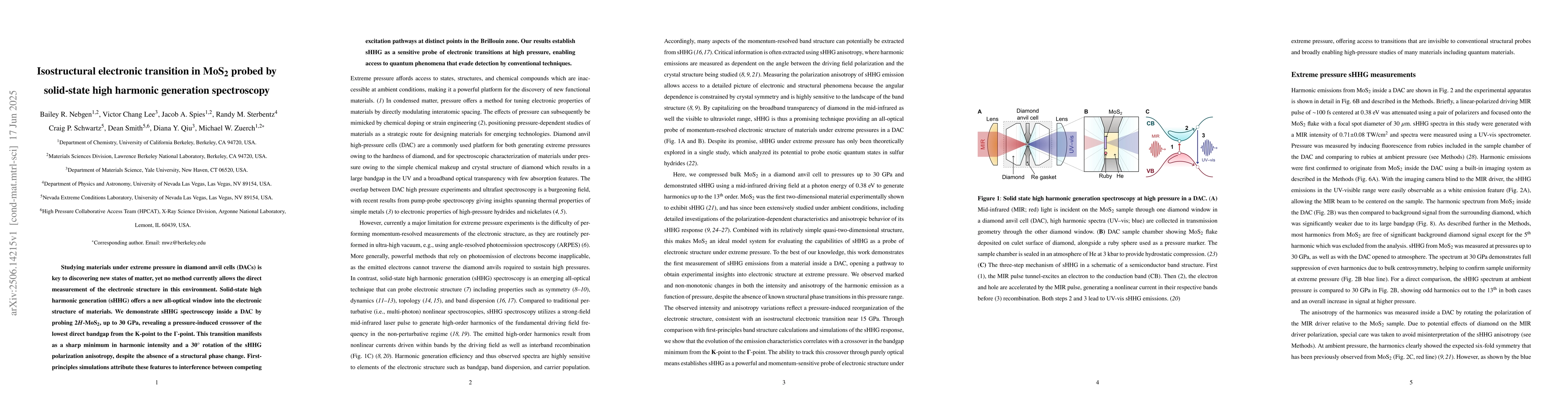
Studying materials under extreme pressure in diamond anvil cells (DACs) is key to discovering new states of matter, yet no method currently allows the direct measurement of the electronic structure in...