ArxivLens
R
Researcher

Robert K. A. Bennett

6 papers on arXiv

6 arXiv Papers
6 Total Publications
Profile

Academic Profile

Name Robert K. A. Bennett
Total Papers 6
Scholar Profile View on Semantic Scholar
Metrics

Statistics

6 arXiv Papers
6 Total Publications
Publications

Papers on arXiv

Thumbnail for Mobility and Threshold Voltage Extraction in Transistors with
  Gate-Voltage-Dependent Contact Resistance
arXiv
Mobility and Threshold Voltage Extraction in Transistors with Gate-Voltage-Dependent Contact Resistance

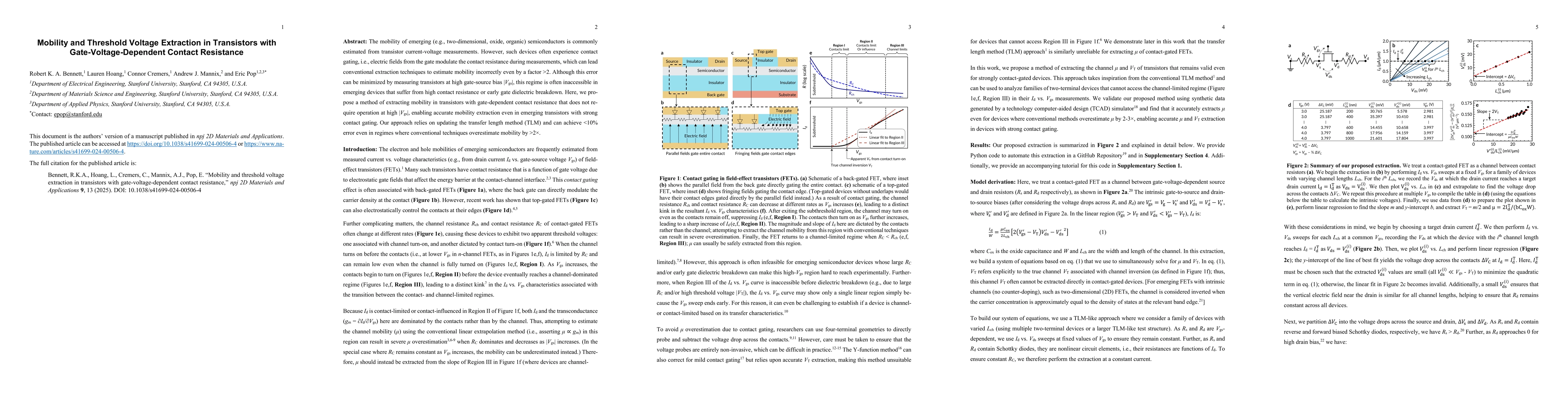
The mobility of emerging (e.g., two-dimensional, oxide, organic) semiconductors is commonly estimated from transistor current-voltage measurements. However, such devices often experience contact gat...

Thumbnail for Biaxial Tensile Strain Enhances Electron Mobility of Monolayer
  Transition Metal Dichalcogenides
arXiv
Biaxial Tensile Strain Enhances Electron Mobility of Monolayer Transition Metal Dichalcogenides

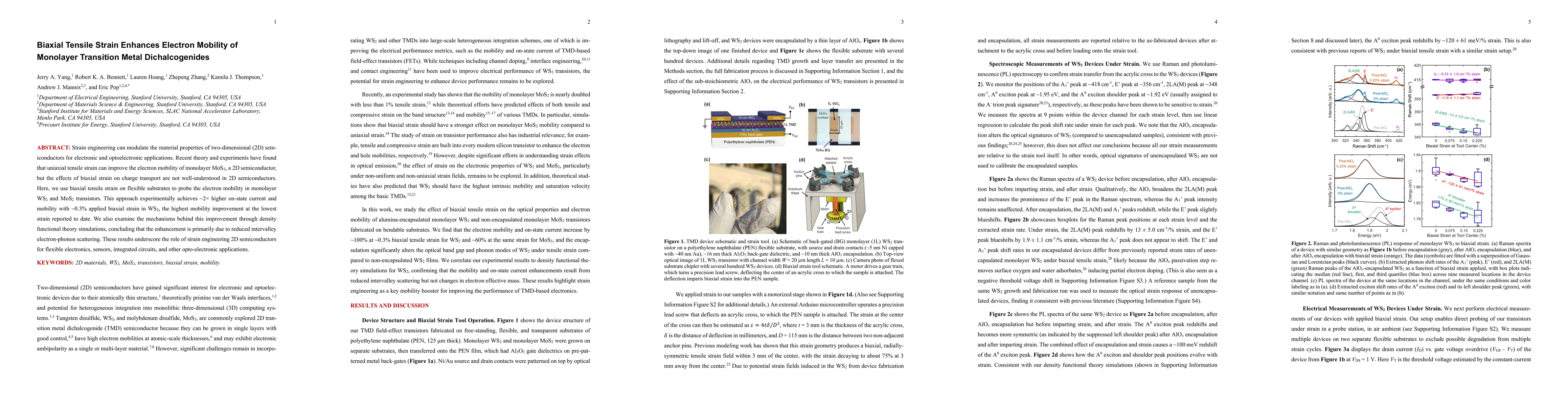
Strain engineering can modulate the material properties of two-dimensional (2D) semiconductors for electronic and optoelectronic applications. Recent theory and experiments have found that uniaxial ...

Thumbnail for How do Quantum Effects Influence the Capacitance and Carrier Density of
  Monolayer MoS$_2$ Transistors?
arXiv
How do Quantum Effects Influence the Capacitance and Carrier Density of Monolayer MoS$_2$ Transistors?

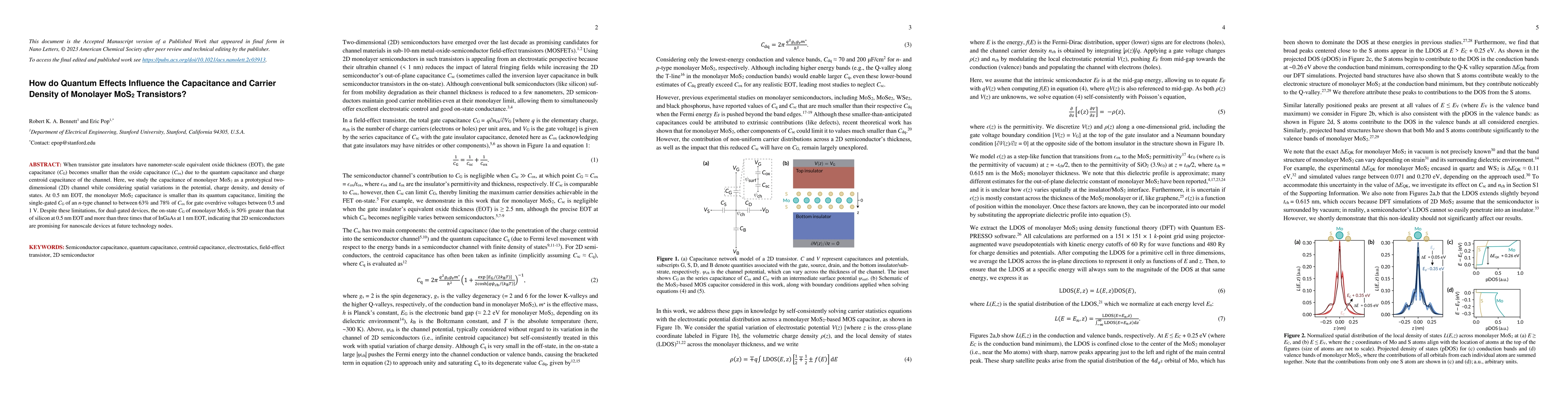
When transistor gate insulators have nanometer-scale equivalent oxide thickness (EOT), the gate capacitance ($C_\textrm{G}$) becomes smaller than the oxide capacitance ($C_\textrm{ox}$) due to the q...

Thumbnail for Enabling P-type Conduction in Bilayer WS2 with NbP Topological Semimetal
  Contacts
arXiv
Enabling P-type Conduction in Bilayer WS2 with NbP Topological Semimetal Contacts

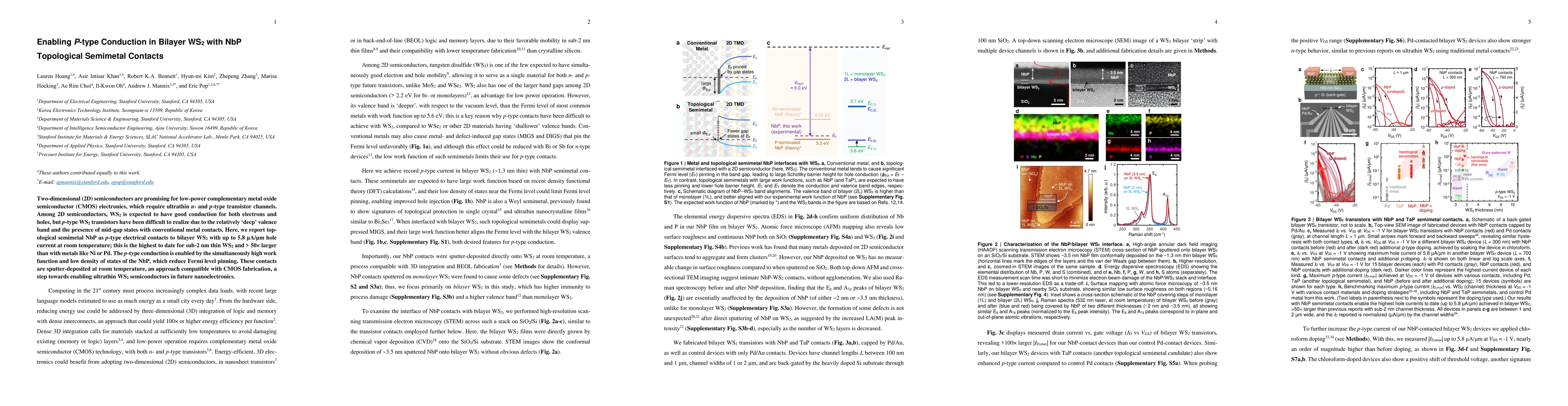
Two-dimensional (2D) semiconductors are promising for low-power complementary metal oxide semiconductor (CMOS) electronics, which require ultrathin n- and p-type transistor channels. Among 2D semicond...

Thumbnail for Low Resistance P-type Contacts to Monolayer WSe$_2$ through Chlorinated
  Solvent Doping
arXiv
Low Resistance P-type Contacts to Monolayer WSe$_2$ through Chlorinated Solvent Doping

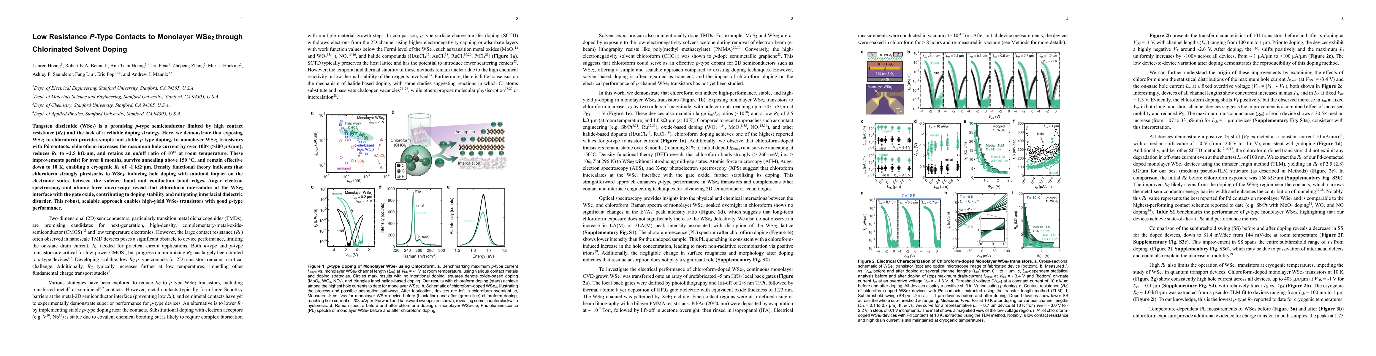
Tungsten diselenide (WSe$_2$) is a promising p-type semiconductor limited by high contact resistance ($R_\textrm{C}$) and the lack of a reliable doping strategy. Here, we demonstrate that exposing WSe...

Thumbnail for Deep Learning to Automate Parameter Extraction and Model Fitting of
  Two-Dimensional Transistors
arXiv
Deep Learning to Automate Parameter Extraction and Model Fitting of Two-Dimensional Transistors

We present a deep learning approach to extract physical parameters (e.g., mobility, Schottky contact barrier height, defect profiles) of two-dimensional (2D) transistors from electrical measurements, ...

This website uses cookies to ensure you get the best experience. Learn more