Academic Profile
Statistics
Similar Authors
Papers on arXiv
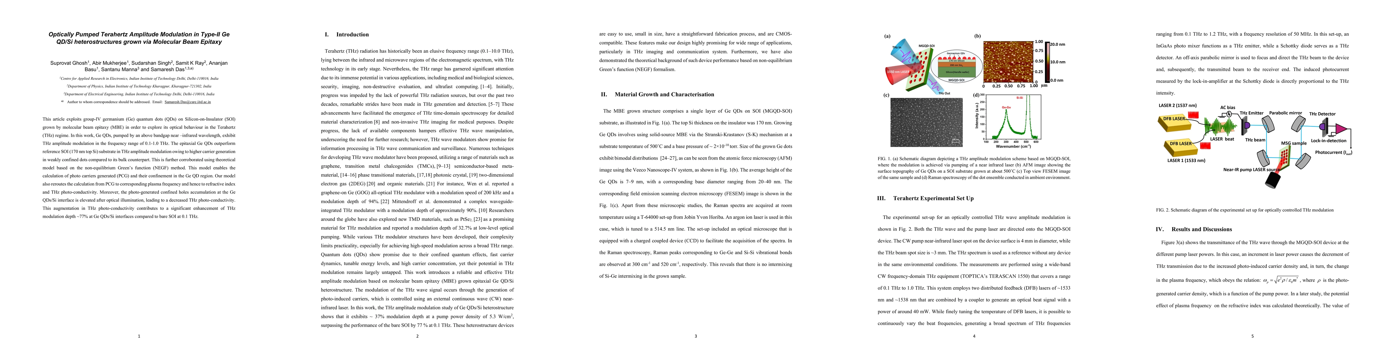
This article exploits group-IV germanium (Ge) quantum dots (QDs) on Silicon-on-Insulator (SOI) grown by molecular beam epitaxy (MBE) in order to explore its optical behaviour in the Terahertz (THz) ...
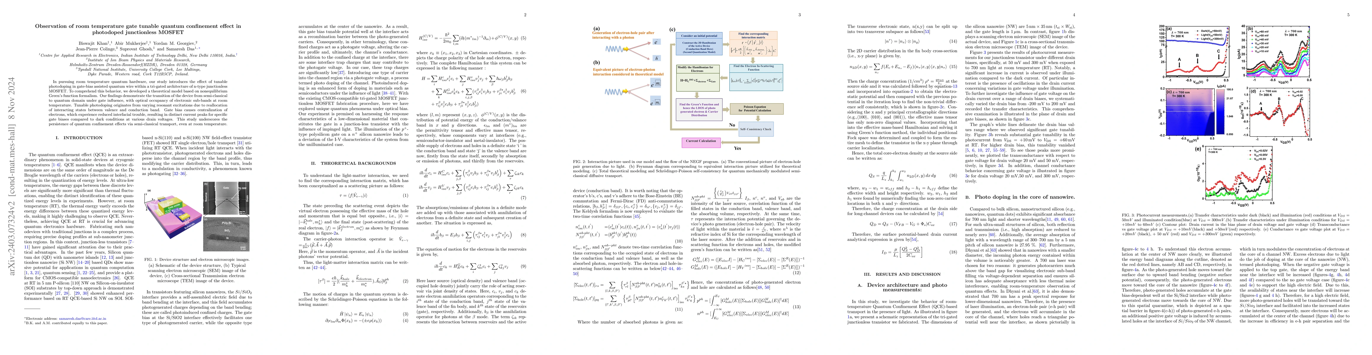
In the pursuit of room temperature quantum hardware, our study introduces a gate voltage tunable quantum wire within a tri-gated n-type junctionless MOSFET. The application of gate voltage alters th...
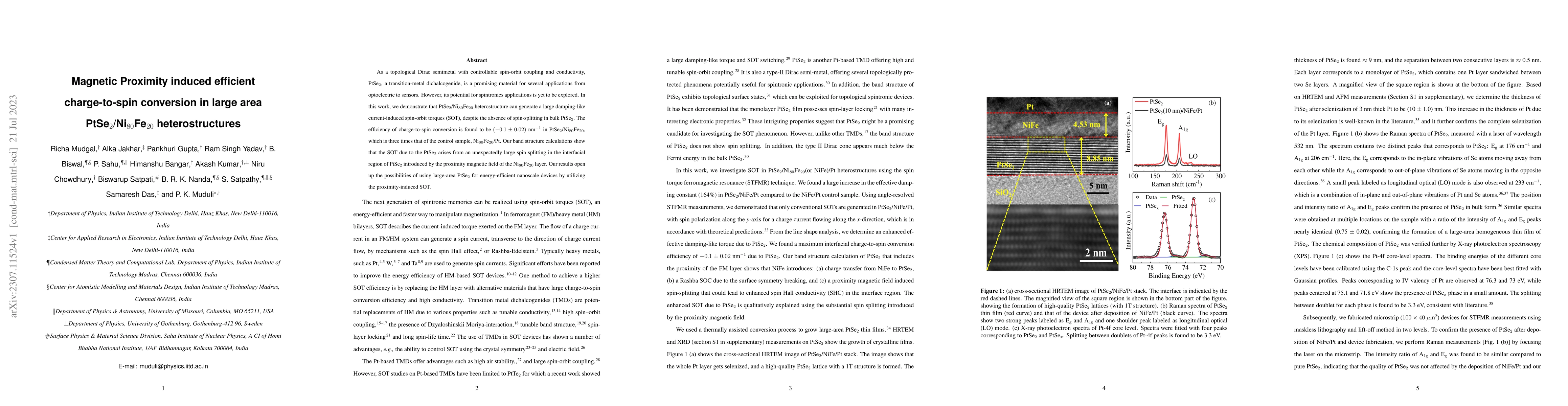
As a topological Dirac semimetal with controllable spin-orbit coupling and conductivity, PtSe$_2$, a transition-metal dichalcogenide, is a promising material for several applications from optoelectr...
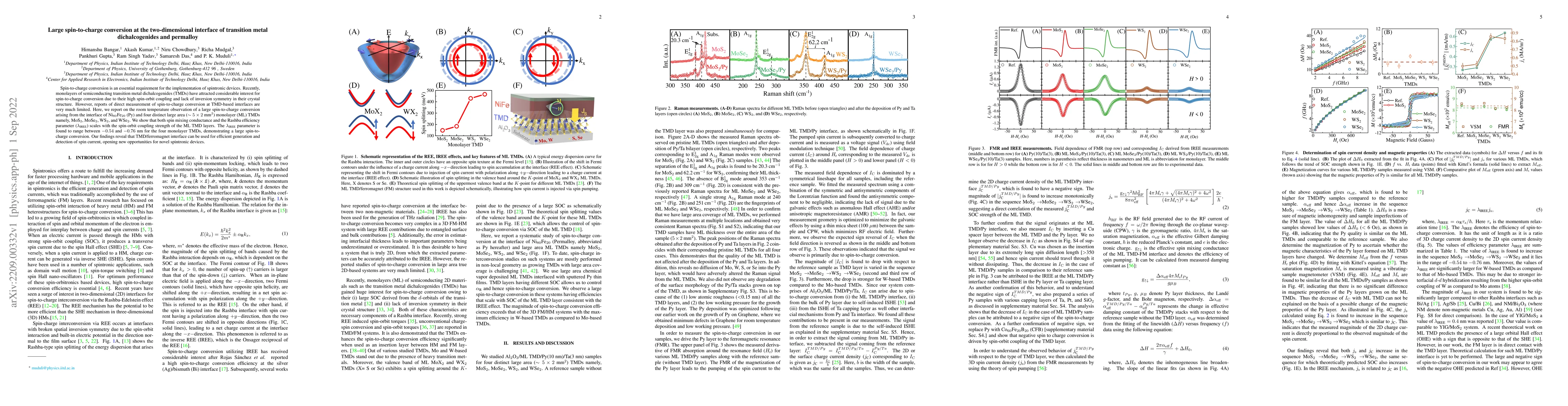
Spin-to-charge conversion is an essential requirement for the implementation of spintronic devices. Recently, monolayers of semiconducting transition metal dichalcogenides (TMDs) have attracted cons...
Recent development on Ge$_{1-x}$Sn$_x$ nanowires with high Sn content, beyond its solid solubility limit, make them attractive for all group-IV Si-integrated infrared photonics at nanoscale. Herein,...
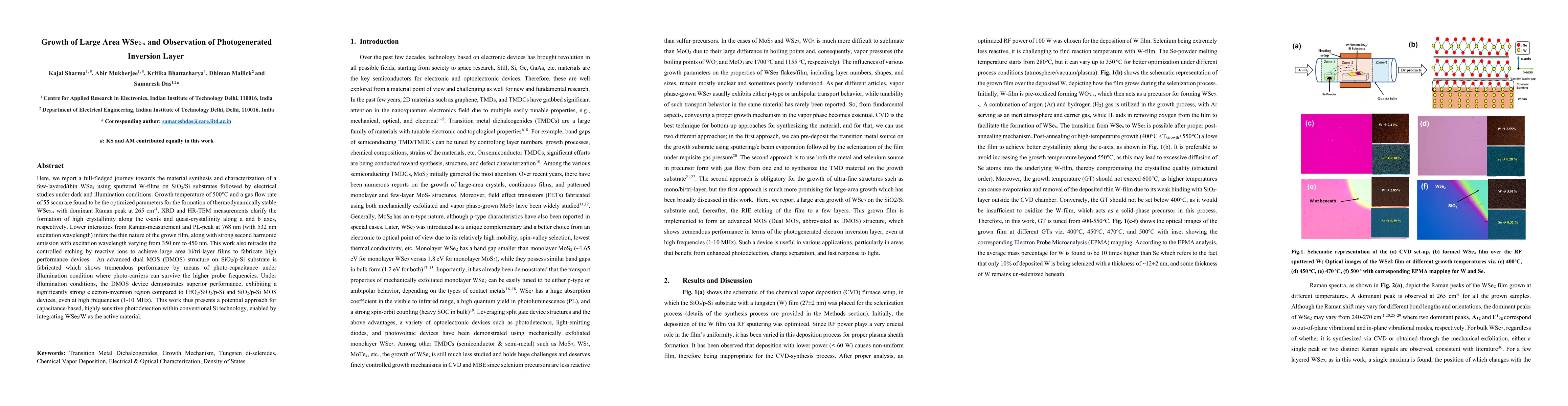
Here, we report the full-fledged journey towards the material synthesis and characterization of few-layered/thin WSe$_2$ using sputtered W-films on SiO$_2$/Si substrates followed by electrical studies...
Achieving low contact resistance in advanced electronic devices remains a significant challenge. As the demand for faster and more energy-efficient devices grows, 2D contact engineering emerges as a p...
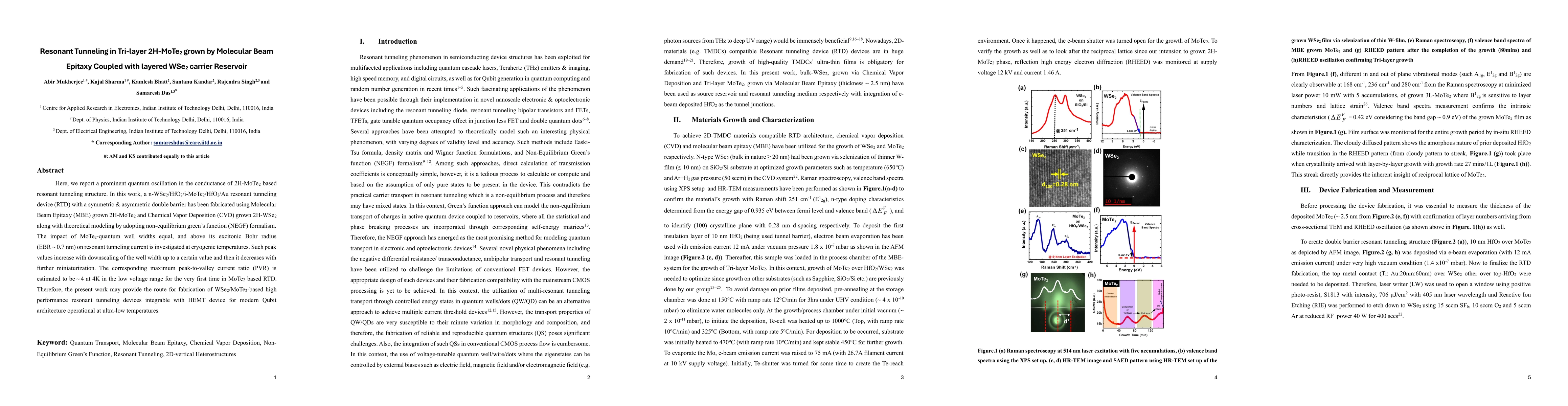
Here, we report a prominent quantum oscillation in the conductance of 2H-MoTe2 based resonant tunneling structure. In this work, a n-WSe2/HfO2/i-MoTe2/HfO2/Au resonant tunneling device (RTD) with a sy...
Recent observations of large unconventional spin-orbit torques in van der Waals (vdW) materials are driving intense interest for energy-efficient spintronic applications. A key limitation of ferromagn...
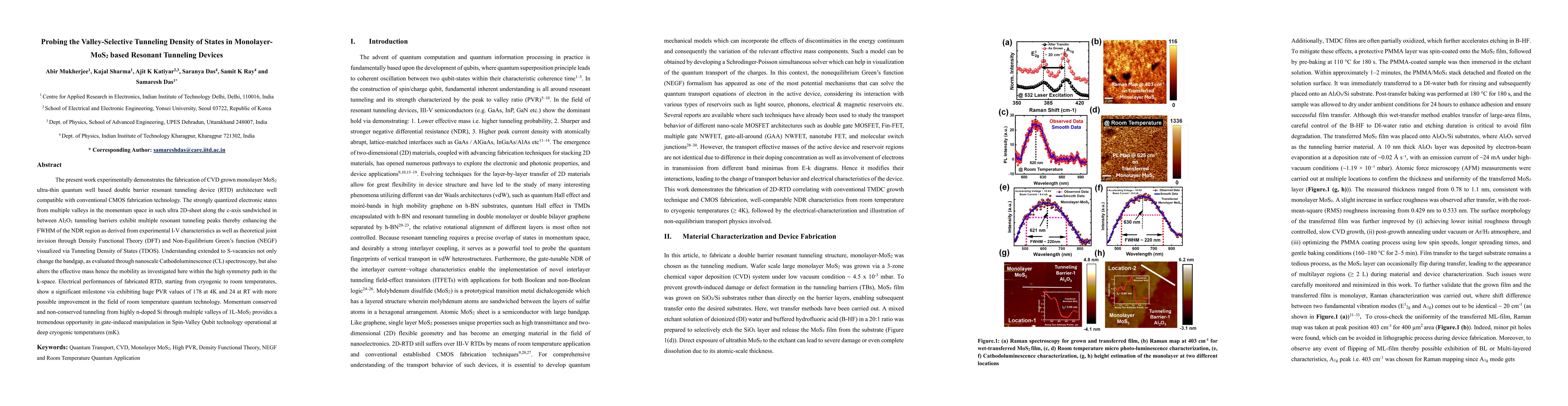
The present work experimentally demonstrates the fabrication of CVD grown monolayer MoS2 ultra thin quantum well based double barrier resonant tunneling device (RTD) architecture well compatible with ...