Academic Profile
Statistics
Similar Authors
Papers on arXiv
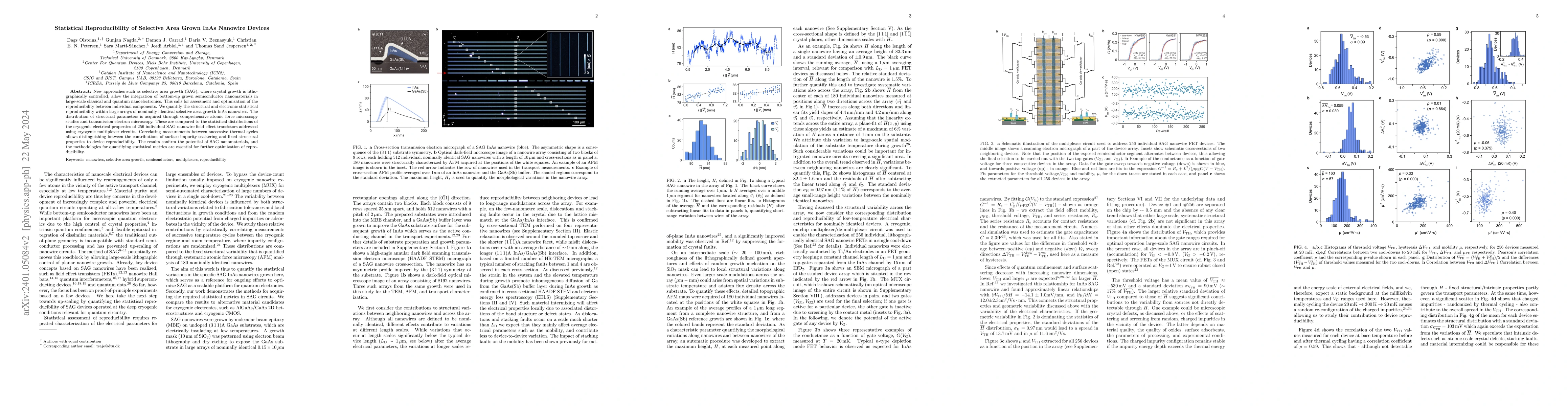
New approaches such as selective area growth, where crystal growth is lithographically controlled, allow the integration of bottom-up grown semiconductor nanomaterials in large-scale classical and q...
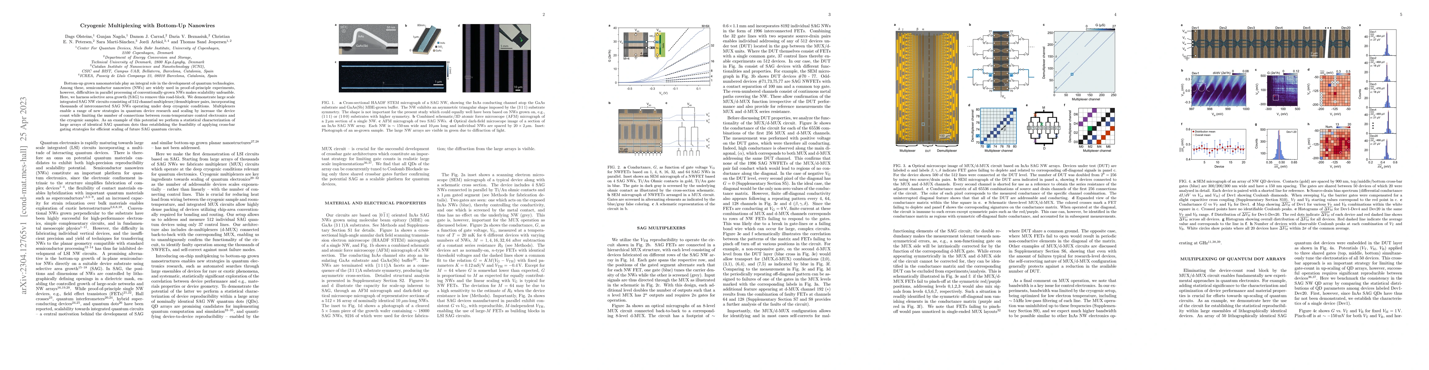
Bottom-up grown nanomaterials play an integral role in the development of quantum technologies. Among these, semiconductor nanowires (NWs) are widely used in proof-of-principle experiments, however,...
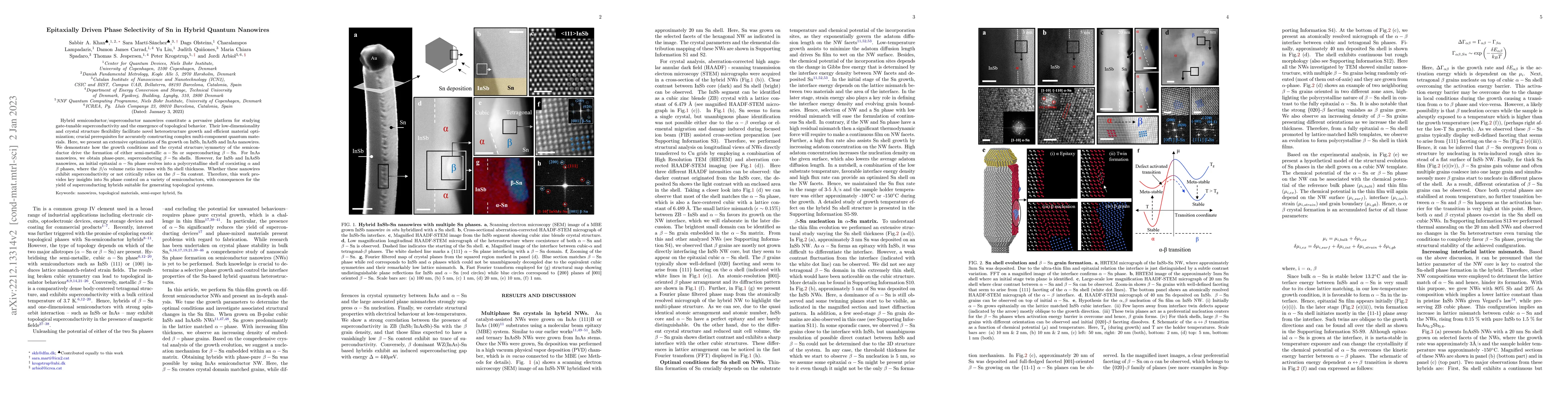
Hybrid semiconductor/superconductor nanowires constitute a pervasive platform for studying gate-tunable superconductivity and the emergence of topological behavior. Their low-dimensionality and crys...
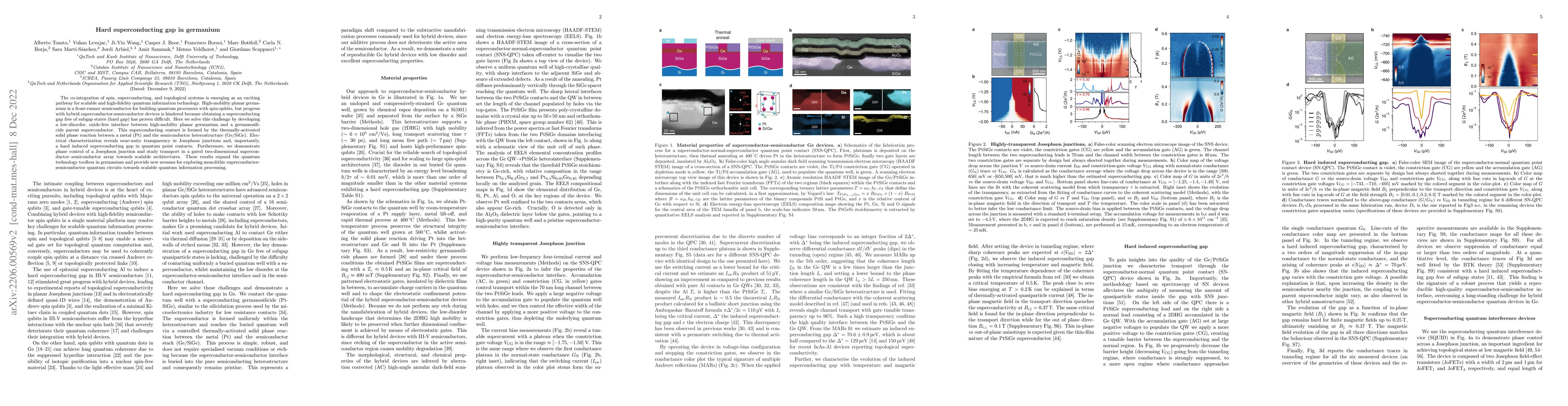
The co-integration of spin, superconducting, and topological systems is emerging as an exciting pathway for scalable and high-fidelity quantum information technology. High-mobility planar germanium ...
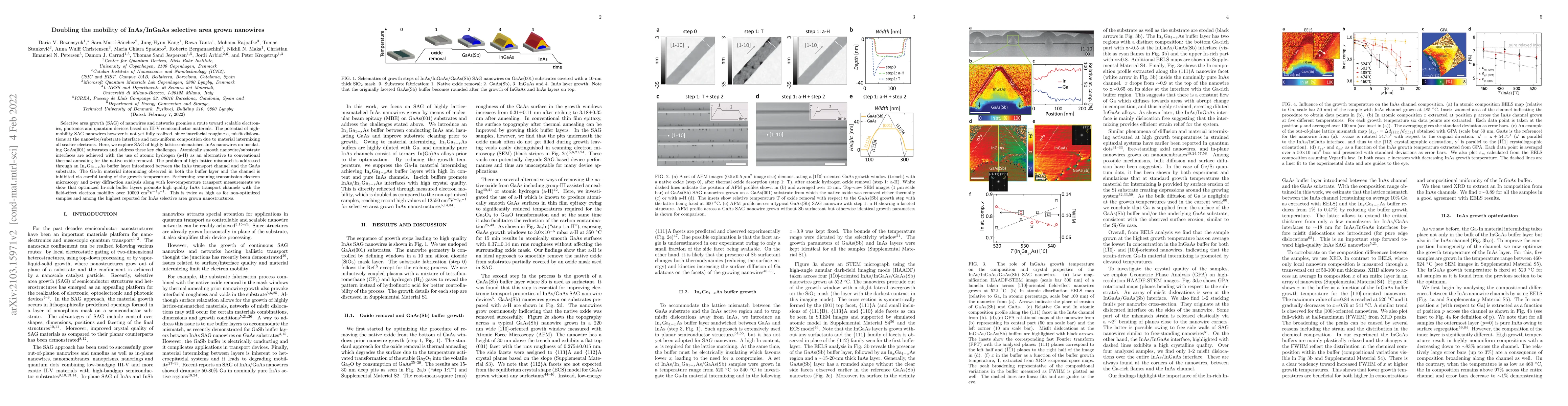
Selective area growth (SAG) of nanowires and networks promise a route toward scalable electronics, photonics and quantum devices based on III-V semiconductor materials. The potential of high-mobilit...
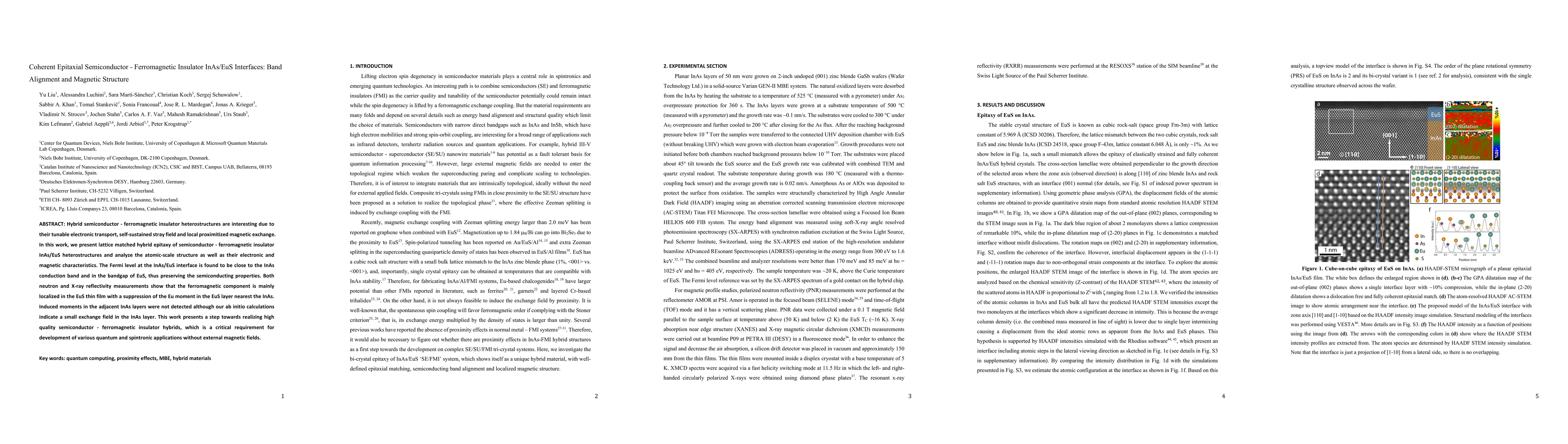
Hybrid semiconductor-ferromagnetic insulator heterostructures are interesting due to their tunable electronic transport, self-sustained stray field and local proximitized magnetic exchange. In this ...
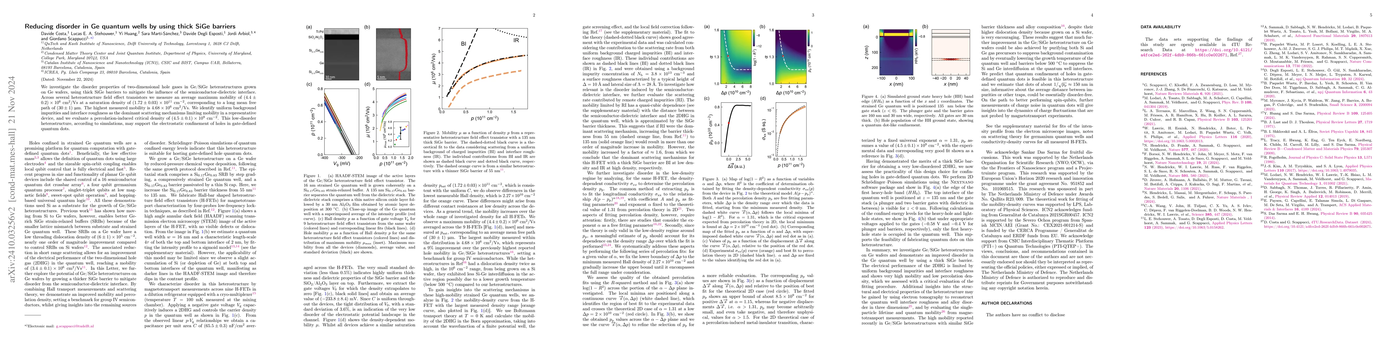
We investigate the disorder properties of two-dimensional hole gases in Ge/SiGe heterostructures grown on Ge wafers, using thick SiGe barriers to mitigate the influence of the semiconductor-dielectric...
This article introduces a groundbreaking analytical workflow designed for the holistic characterisation, modelling and physical simulation of device heterostructures. Our innovative workflow autonomou...
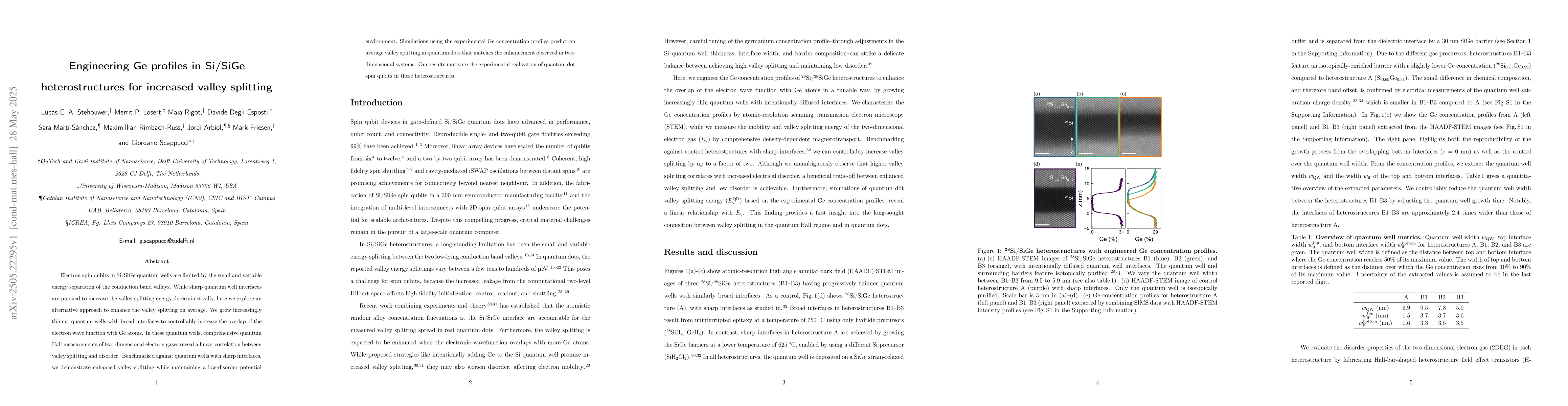
Electron spin qubits in Si/SiGe quantum wells are limited by the small and variable energy separation of the conduction band valleys. While sharp quantum well interfaces are pursued to increase the va...
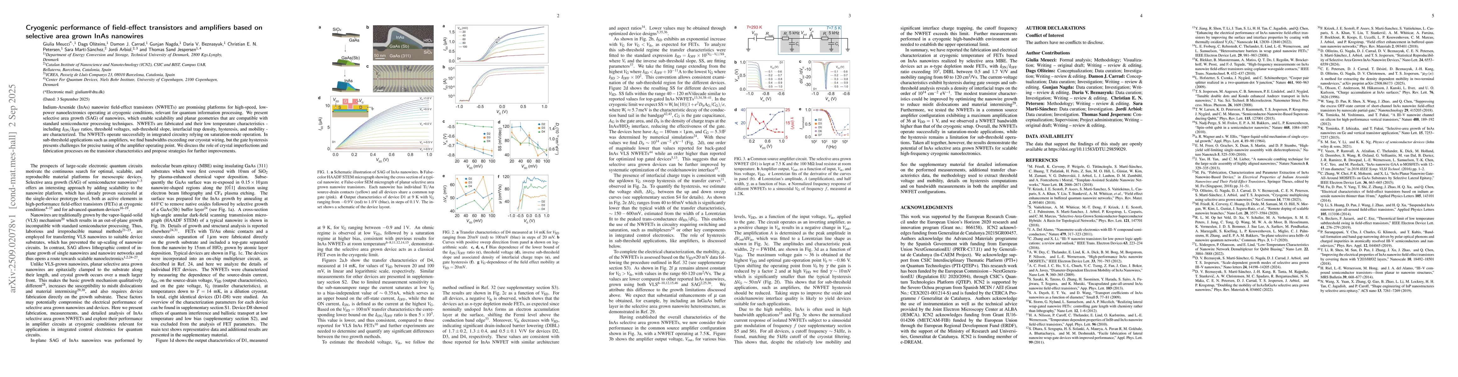
Indium-Arsenide (InAs) nanowire field-effect transistors (NWFETs) are promising platforms for high-speed, low power nanoelectronics operating at cryogenic conditions, relevant for quantum information ...