ArxivLens
S
Researcher

Sarah J. Haigh

23 papers on arXiv

23 arXiv Papers
32 Total Publications
Profile

Academic Profile

Name Sarah J. Haigh
Total Papers 32
Scholar Profile View on Semantic Scholar
Metrics

Statistics

23 arXiv Papers
32 Total Publications
Publications

Papers on arXiv

Thumbnail for Ultra-clean assembly of van der Waals heterostructures
arXiv
Ultra-clean assembly of van der Waals heterostructures

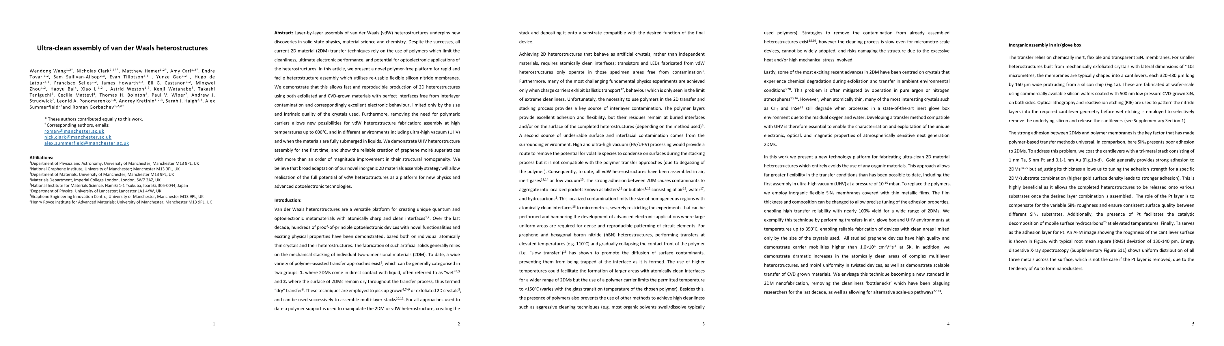
Layer-by-layer assembly of van der Waals (vdW) heterostructures underpins new discoveries in solid state physics, material science and chemistry. Despite the successes, all current 2D material (2DM)...

Thumbnail for Highly ${ }^{28} \mathrm{Si}$ Enriched Silicon by Localised Focused Ion
  Beam Implantation
arXiv
Highly ${ }^{28} \mathrm{Si}$ Enriched Silicon by Localised Focused Ion Beam Implantation

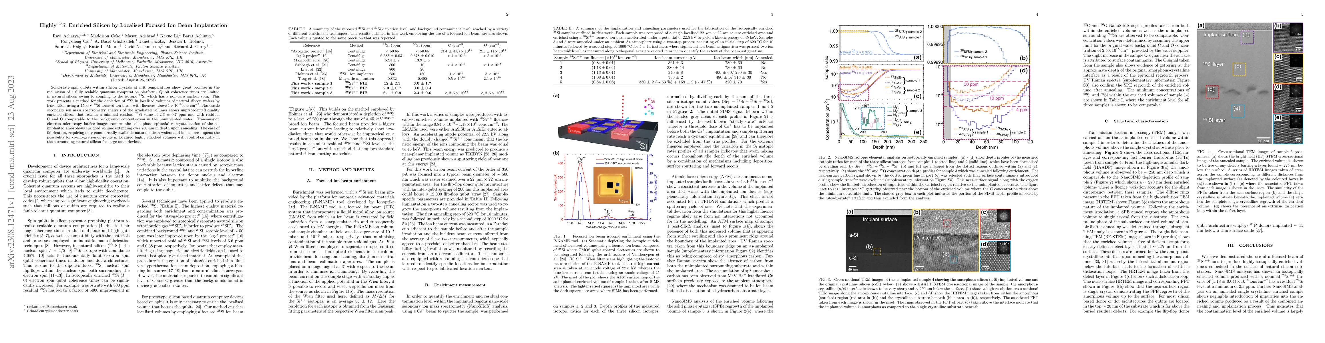
Solid-state spin qubits within silicon crystals at mK temperatures show great promise in the realisation of a fully scalable quantum computation platform. Qubit coherence times are limited in natura...

Thumbnail for Telluride nanocrystals with adjustable amorphous shell thickness and
  core-shell structure modulation by aqueous cation-exchange
arXiv
Telluride nanocrystals with adjustable amorphous shell thickness and core-shell structure modulation by aqueous cation-exchange

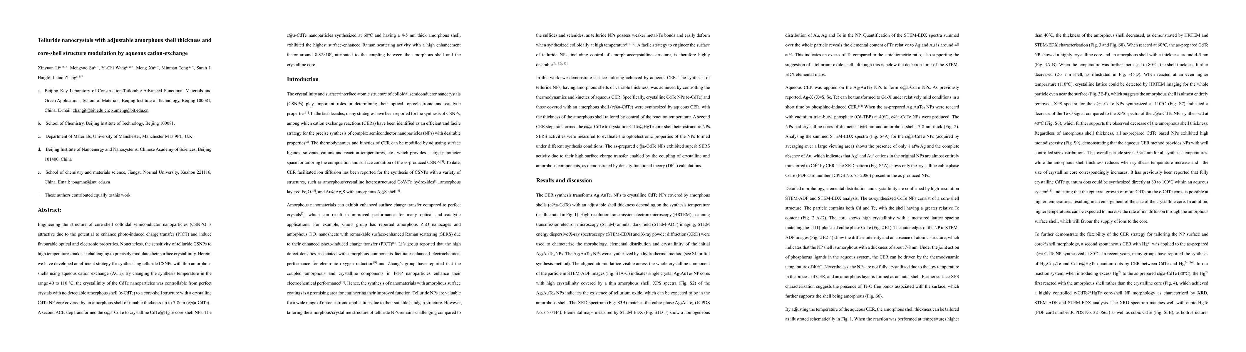
Engineering the structure of core-shell colloidal semiconductor nanoparticles (CSNPs) is attractive due to the potential to enhance photo-induced charge transfer (PICT) and induce favourable optical...

Thumbnail for Tracking single atoms in a liquid environment
arXiv
Tracking single atoms in a liquid environment

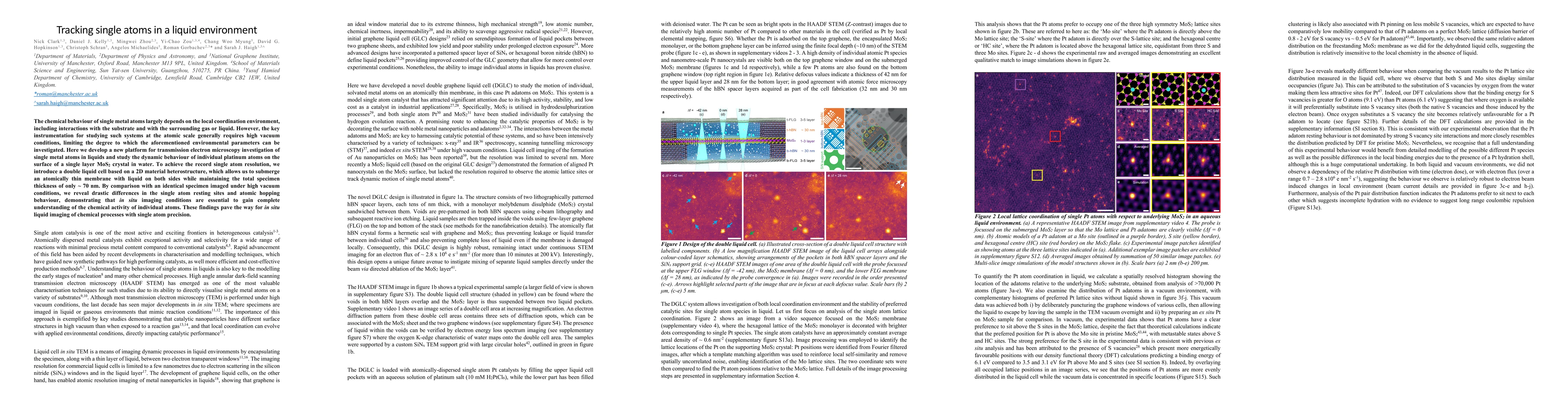
The chemical behaviour of single metal atoms largely depends on the local coordination environment, including interactions with the substrate and with the surrounding gas or liquid. However, the key...

Thumbnail for Surfactant-Free Synthesis of Spiky Hollow Ag-Au Nanostars with
  Chemically Exposed Surfaces for Enhanced Catalysis and Single-Particle SERS
arXiv
Surfactant-Free Synthesis of Spiky Hollow Ag-Au Nanostars with Chemically Exposed Surfaces for Enhanced Catalysis and Single-Particle SERS

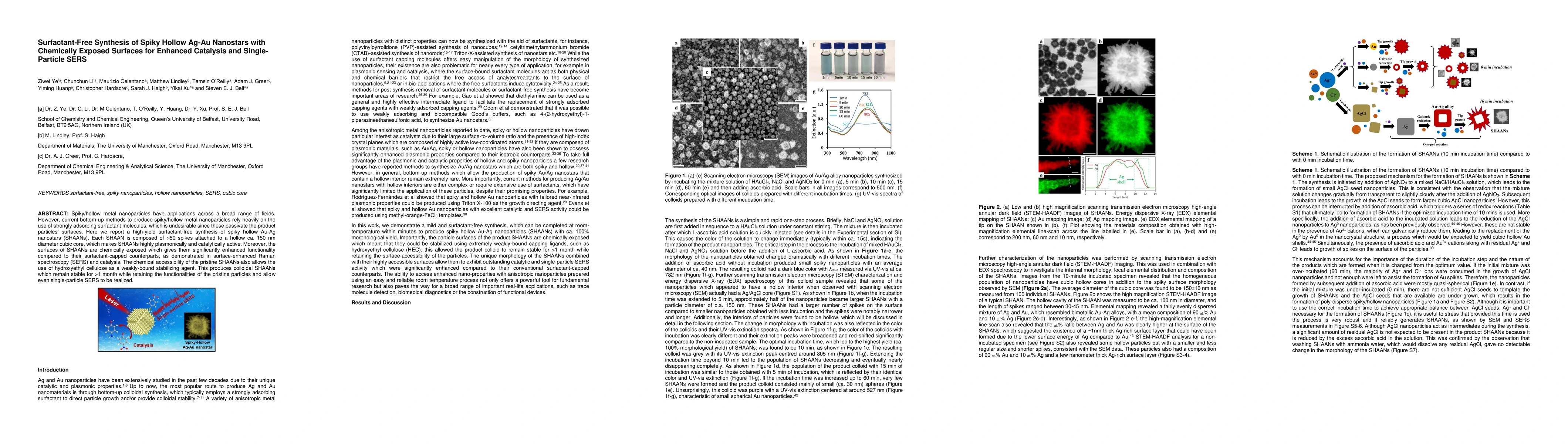
Spiky/hollow metal nanoparticles have applications across a broad range of fields. However, current bottom-up methods to produce spiky/hollow metal nanoparticles rely heavily on the use of strongly ...

Thumbnail for Doped graphene/carbon black hybrid catalyst giving enhanced oxygen
  reduction reaction activity with high resistance to corrosion in proton
  exchange membrane fuel cells
arXiv
Doped graphene/carbon black hybrid catalyst giving enhanced oxygen reduction reaction activity with high resistance to corrosion in proton exchange membrane fuel cells

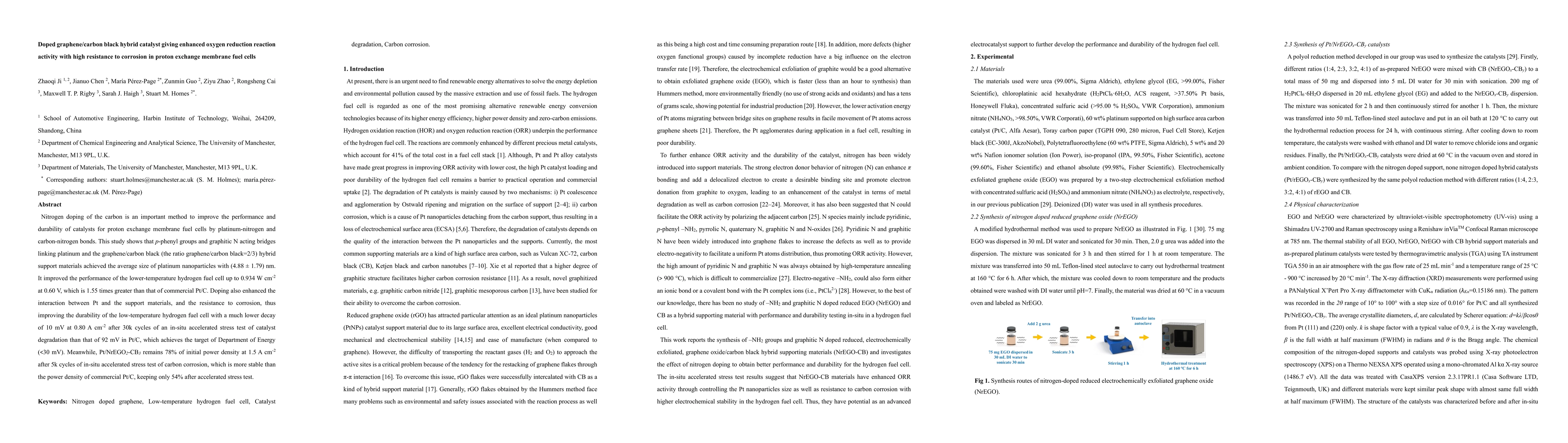
Nitrogen doping of the carbon is an important method to improve the performance and durability of catalysts for proton exchange membrane fuel cells by platinum-nitrogen and carbon-nitrogen bonds. Th...

Thumbnail for Interfacial ferroelectricity in marginally twisted 2D semiconductors
arXiv
Interfacial ferroelectricity in marginally twisted 2D semiconductors

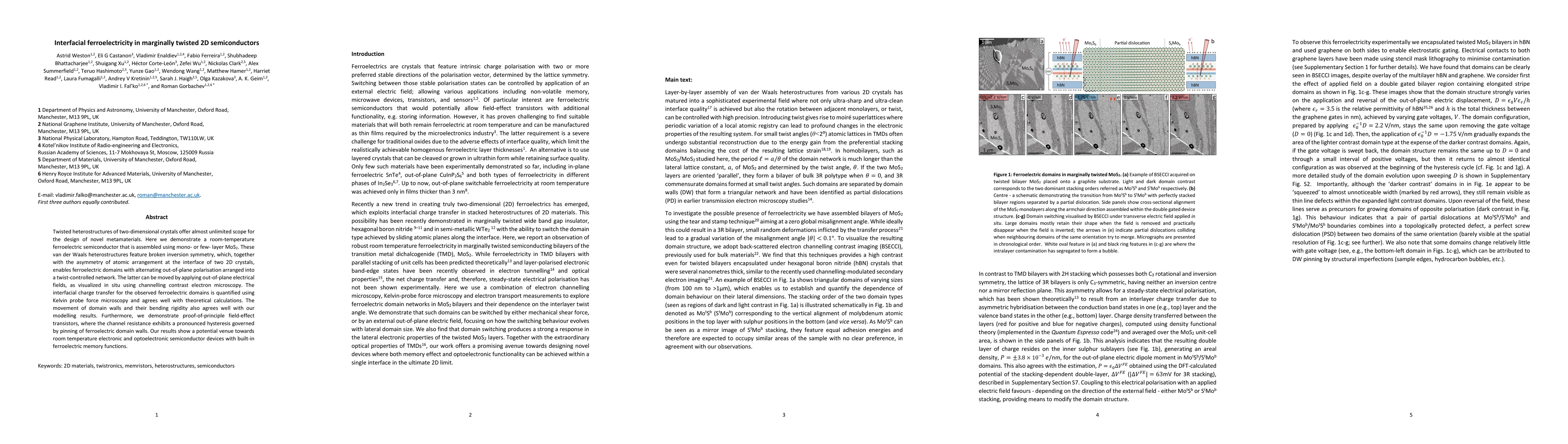
Twisted heterostructures of two-dimensional crystals offer almost unlimited scope for the design of novel metamaterials. Here we demonstrate a room-temperature ferroelectric semiconductor that is as...

Thumbnail for Ion exchange in atomically thin clays and micas
arXiv
Ion exchange in atomically thin clays and micas

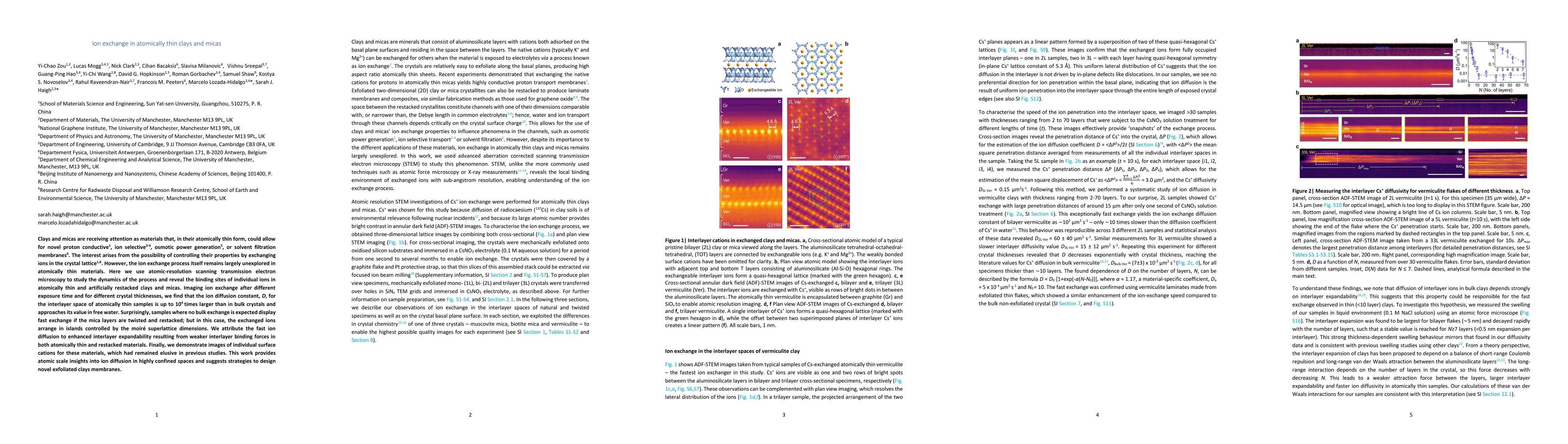
Clays and micas are receiving attention as materials that, in their atomically thin form, could allow for novel proton conductive, ion selective, osmotic power generation, or solvent filtration memb...

Thumbnail for Atomic Resolution Imaging of CrBr$_{3}$ using Adhesion-Enhanced Grids
arXiv
Atomic Resolution Imaging of CrBr$_{3}$ using Adhesion-Enhanced Grids

Suspended specimens of 2D crystals and their heterostructures are required for a range of studies including transmission electron microscopy (TEM), optical transmission experiments and nanomechanica...

Thumbnail for Holographic reconstruction of the interlayer distance of bilayer
  two-dimensional crystal samples from their convergent beam electron
  diffraction patterns
arXiv
Holographic reconstruction of the interlayer distance of bilayer two-dimensional crystal samples from their convergent beam electron diffraction patterns

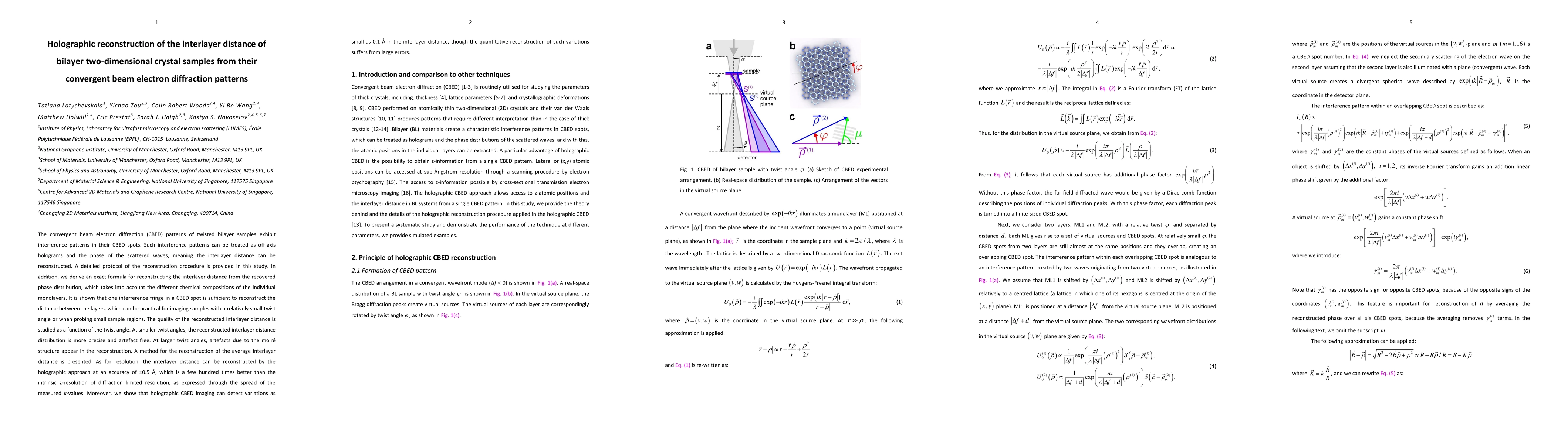
The convergent beam electron diffraction (CBED) patterns of twisted bilayer samples exhibit interference patterns in their CBED spots. Such interference patterns can be treated as off-axis holograms...

Thumbnail for Raman Fingerprints of Graphene Produced by Anodic Electrochemical
  Exfoliation
arXiv
Raman Fingerprints of Graphene Produced by Anodic Electrochemical Exfoliation

Electrochemical exfoliation is one of the most promising methods for scalable production of graphene. However, limited understanding of its Raman spectrum as well as lack of measurement standards fo...

Thumbnail for Convergent beam electron diffraction of multilayer van der Waals
  structures
arXiv
Convergent beam electron diffraction of multilayer van der Waals structures

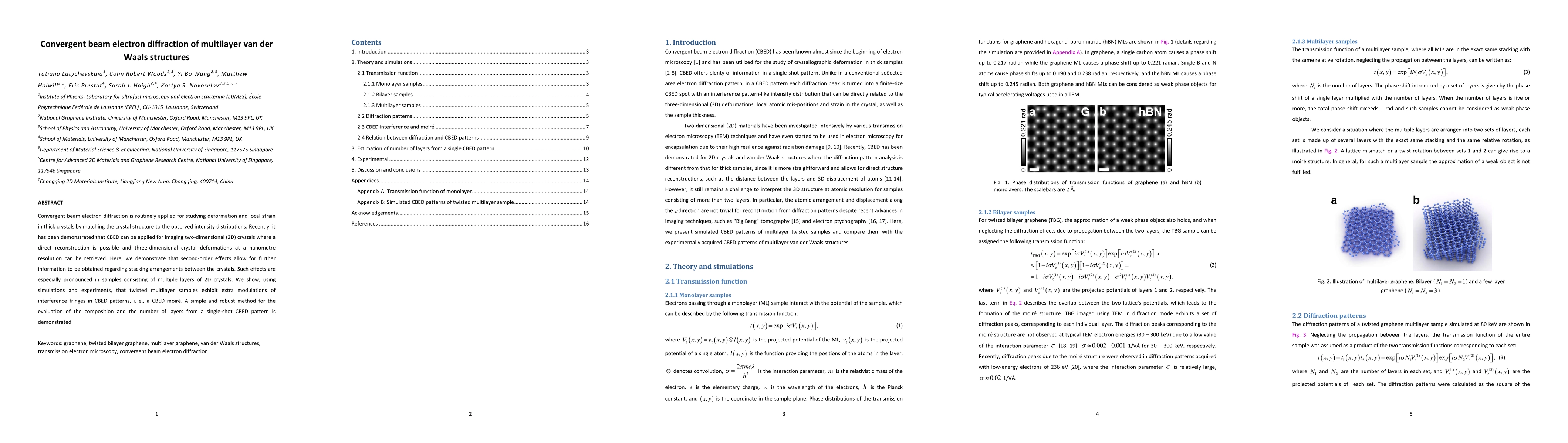
Convergent beam electron diffraction is routinely applied for studying deformation and local strain in thick crystals by matching the crystal structure to the observed intensity distributions. Recen...

Thumbnail for Stacking Order in Graphite Films Controlled by Van der Waals Technology
arXiv
Stacking Order in Graphite Films Controlled by Van der Waals Technology

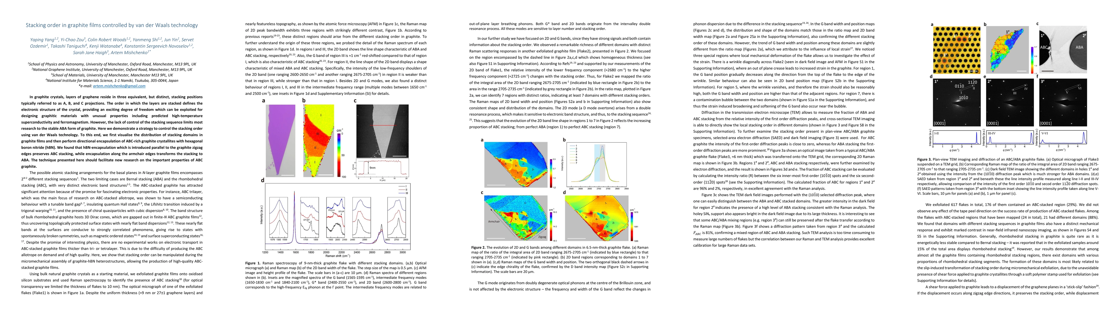
In graphite crystals, layers of graphene reside in three equivalent, but distinct, stacking positions typically referred to as A, B, and C projections. The order in which the layers are stacked defi...

Thumbnail for Two-dimensional covalent crystals by chemical conversion of thin van der
  Waals materials
arXiv
Two-dimensional covalent crystals by chemical conversion of thin van der Waals materials

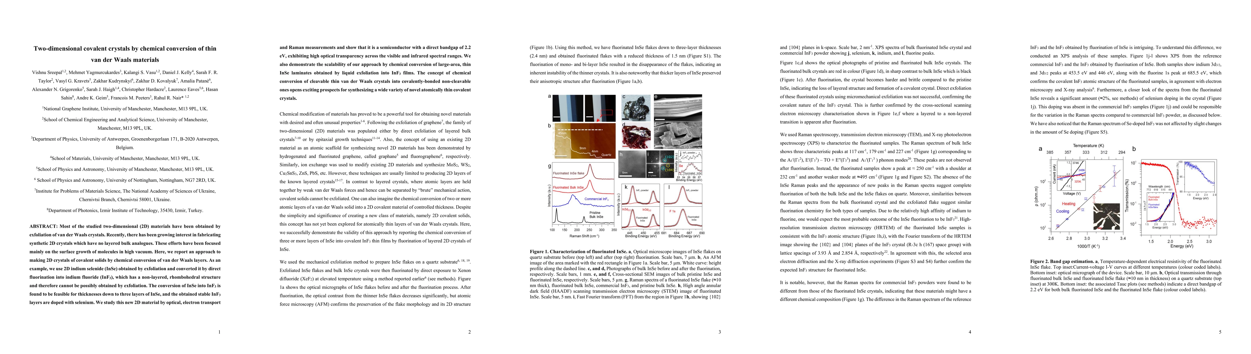
Most of the studied two-dimensional (2D) materials have been obtained by exfoliation of van der Waals crystals. Recently, there has been growing interest in fabricating synthetic 2D crystals which h...

Thumbnail for Self-limiting growth of two-dimensional palladium between graphene oxide
  layers
arXiv
Self-limiting growth of two-dimensional palladium between graphene oxide layers

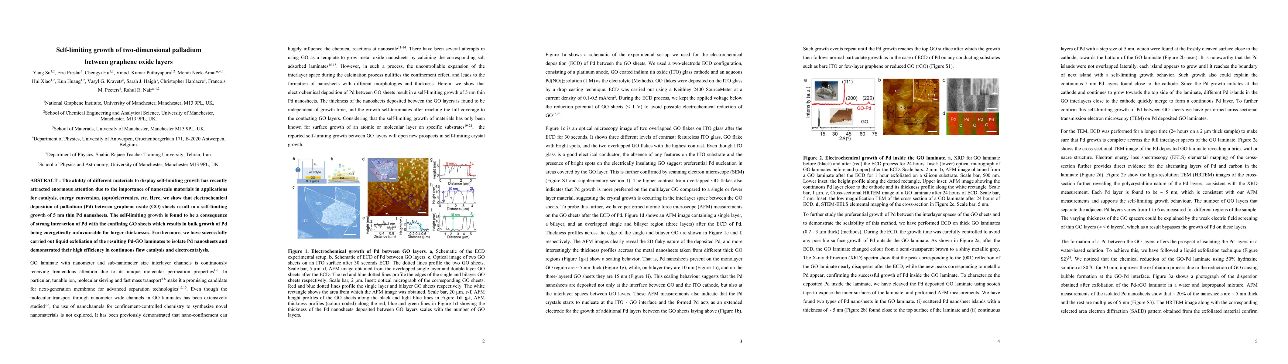
The ability of different materials to display self-limiting growth has recently attracted enormous attention due to the importance of nanoscale materials in applications for catalysis, energy conver...

Thumbnail for One-step synthesis of graphene containing topological defects
arXiv
One-step synthesis of graphene containing topological defects

Chemical vapour deposition enables large-domain growth of ideal graphene, yet many applications of graphene require the controlled inclusion of specific defects. We present a one-step chemical vapour ...

Thumbnail for Production of Ultra-Thin and High-Quality Nanosheet Networks via
  Layer-by-Layer Assembly at Liquid-Liquid Interfaces
arXiv
Production of Ultra-Thin and High-Quality Nanosheet Networks via Layer-by-Layer Assembly at Liquid-Liquid Interfaces

Solution-processable 2D materials are promising candidates for a range of printed electronics applications. Yet maximising their potential requires solution-phase processing of nanosheets into high-qu...

Thumbnail for Electron Channelling Contrast SEM Imaging of Twist Domains in Transition
  Metal Dichalcogenide Heterostructures
arXiv
Electron Channelling Contrast SEM Imaging of Twist Domains in Transition Metal Dichalcogenide Heterostructures

Twisted 2D material heterostructures provide an exciting platform for investigating new fundamental physical phenomena. Many of the most interesting behaviours emerge at small twist angles, where the ...

Thumbnail for Dynamics of single Au nanoparticles on graphene simultaneously in real-
  and diffraction space by time-series convergent beam electron diffraction
arXiv
Dynamics of single Au nanoparticles on graphene simultaneously in real- and diffraction space by time-series convergent beam electron diffraction

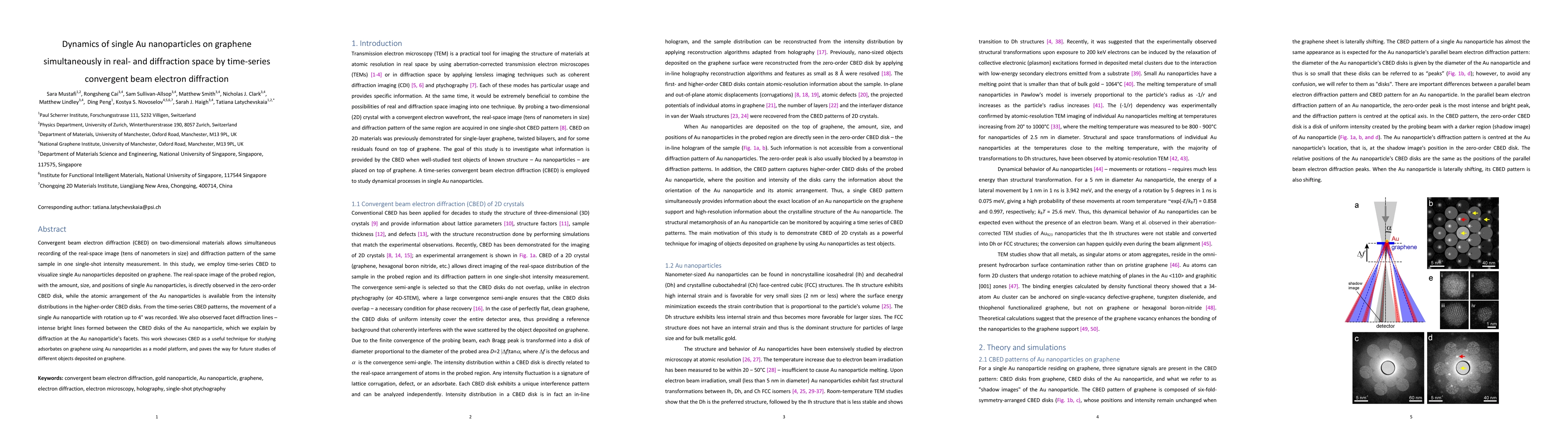
Convergent beam electron diffraction (CBED) on two-dimensional materials allows simultaneous recording of the real-space image (tens of nanometers in size) and diffraction pattern of the same sample i...

Thumbnail for Bulk Ferroelectric Heterostructures for High Temperature Lead-Free
  Piezoelectrics
arXiv
Bulk Ferroelectric Heterostructures for High Temperature Lead-Free Piezoelectrics

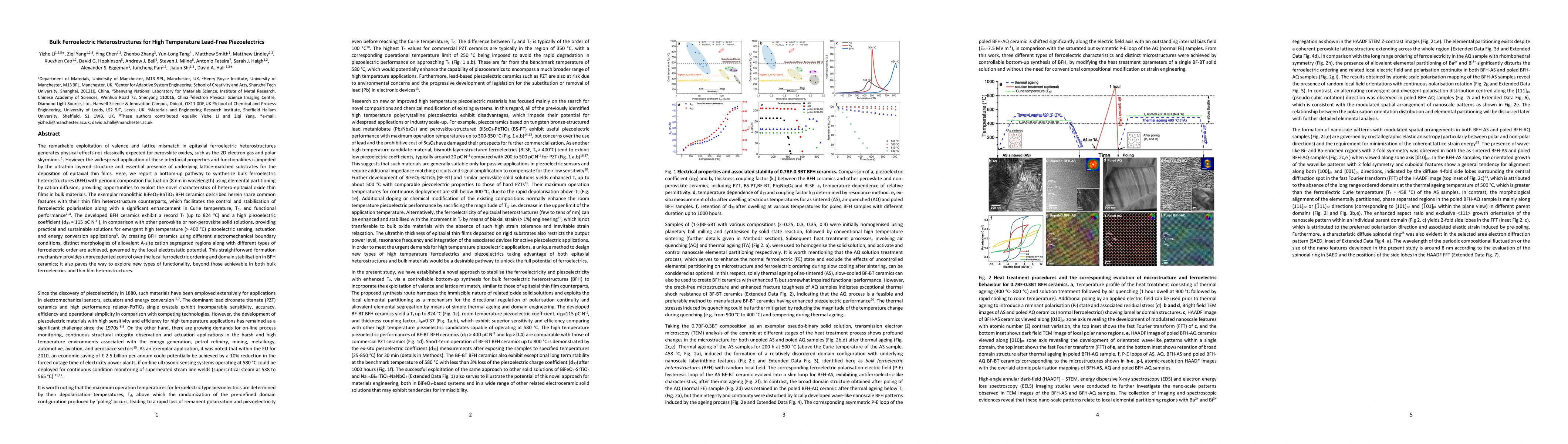
Remarkable exploitation of valence and lattice mismatch in epitaxial ferroelectric heterostructures generates physical effects not classically expected for perovskite oxides, such as 2D electron gas a...

Thumbnail for Noise2Void for Denoising Atomic Resolution Scanning Transmission Electron Microscopy Images
arXiv
Noise2Void for Denoising Atomic Resolution Scanning Transmission Electron Microscopy Images

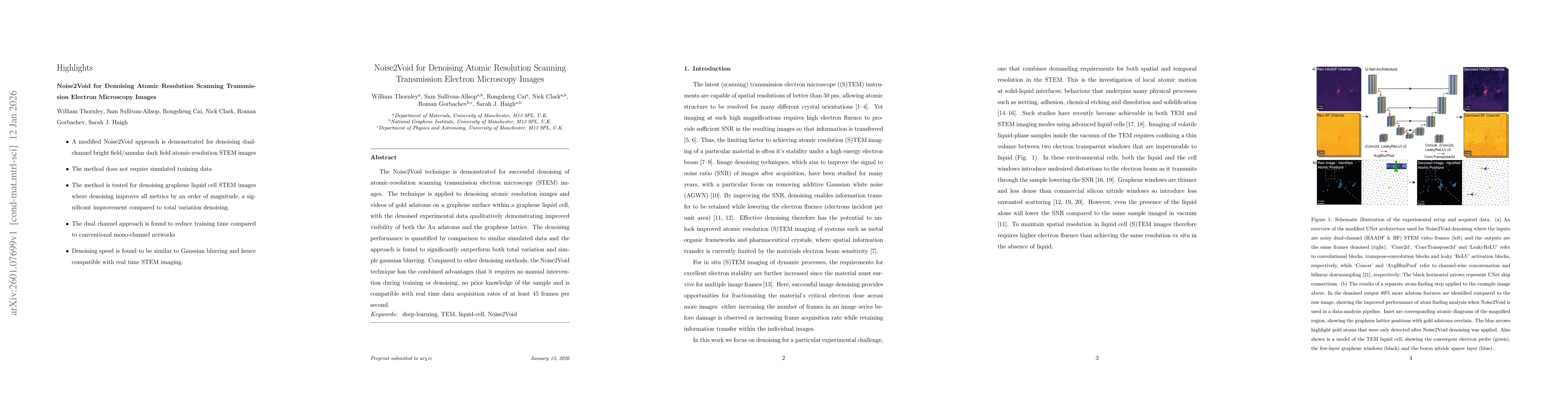
The Noise2Void technique is demonstrated for successful denoising of atomic-resolution scanning transmission electron microscopy (STEM) images. The technique is applied to denoising atomic resolution ...

Thumbnail for Atomic imaging of 2D transition metal dihalides
arXiv
Atomic imaging of 2D transition metal dihalides

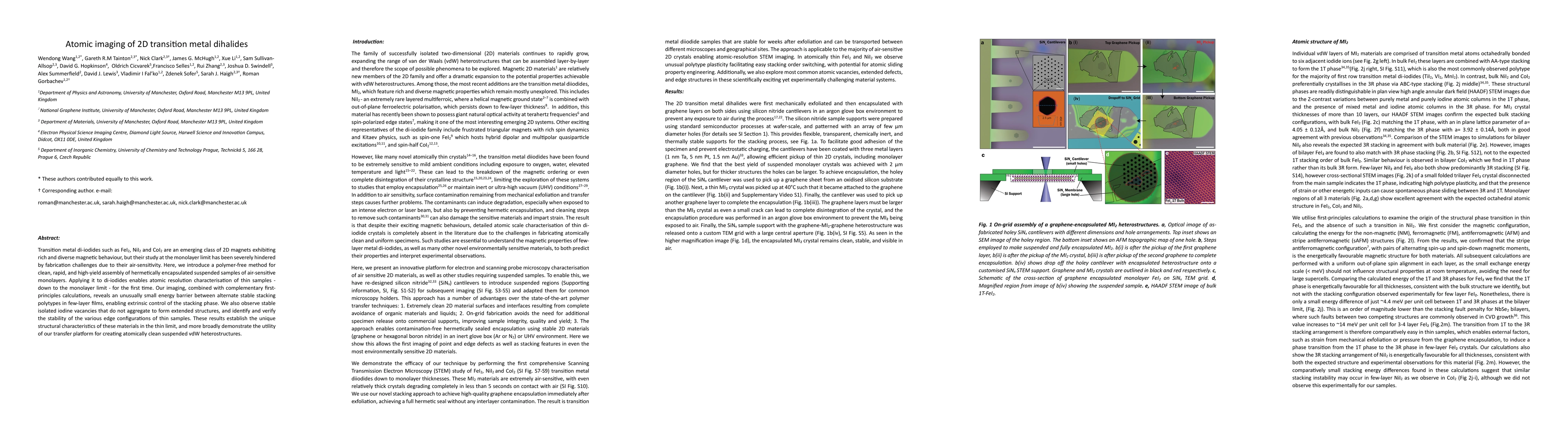
Transition metal di-iodides such as FeI2, NiI2 and CoI2 are an emerging class of 2D magnets exhibiting rich and diverse magnetic behaviour, but their study at the monolayer limit has been severely hin...

Thumbnail for Atomic-resolution imaging of gold species at organic liquid-solid interfaces
arXiv
Atomic-resolution imaging of gold species at organic liquid-solid interfaces

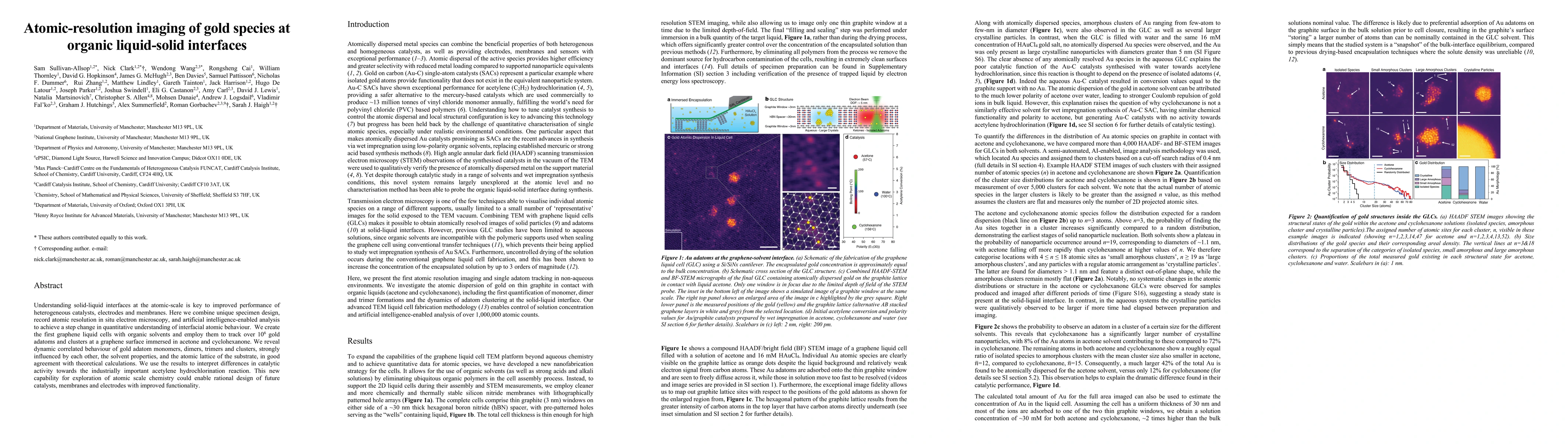
Understanding solid-liquid interfaces at the atomic-scale is key to improved performance of heterogeneous catalysts, electrodes and membranes. Here we combine unique specimen design, record atomic res...

This website uses cookies to ensure you get the best experience. Learn more