Academic Profile
Statistics
Similar Authors
Papers on arXiv
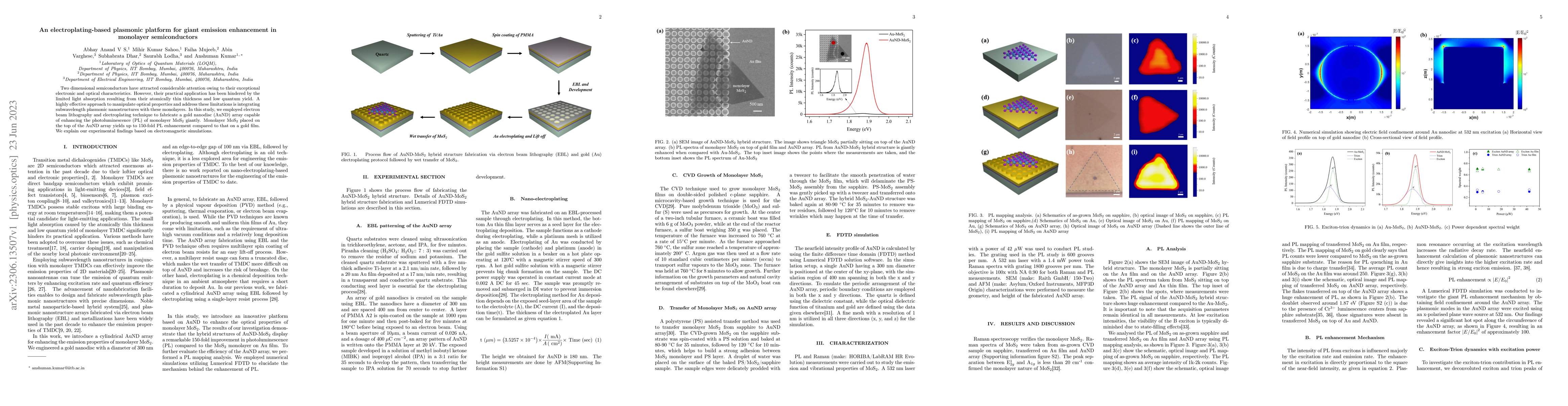
Two dimensional semiconductors have attracted considerable attention owing to their exceptional electronic and optical characteristics. However, their practical application has been hindered by the ...
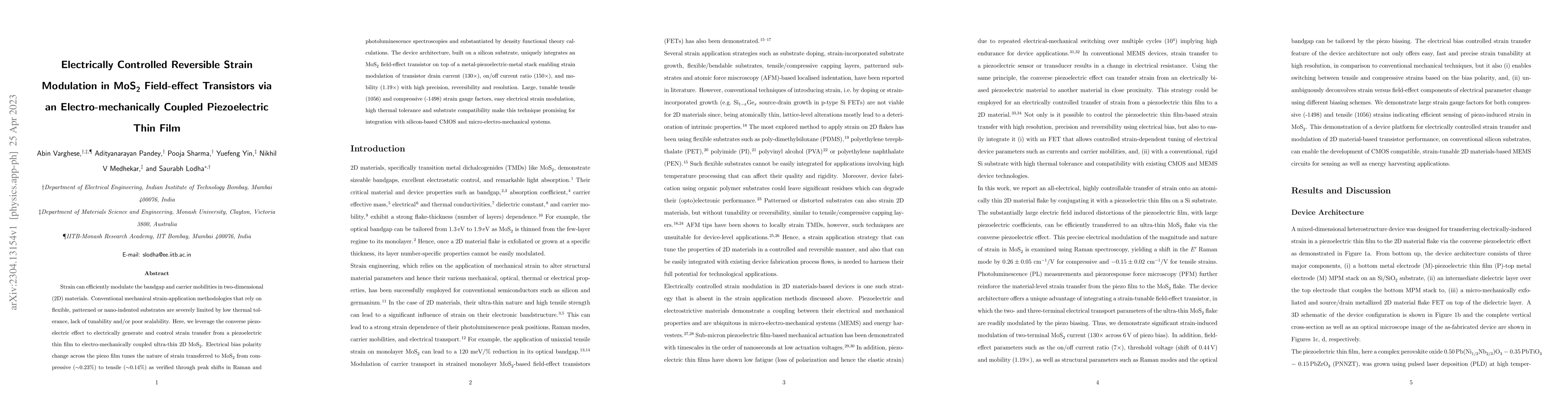
Strain can efficiently modulate the bandgap and carrier mobilities in two-dimensional (2D) materials. Conventional mechanical strain-application methodologies that rely on flexible, patterned or nan...
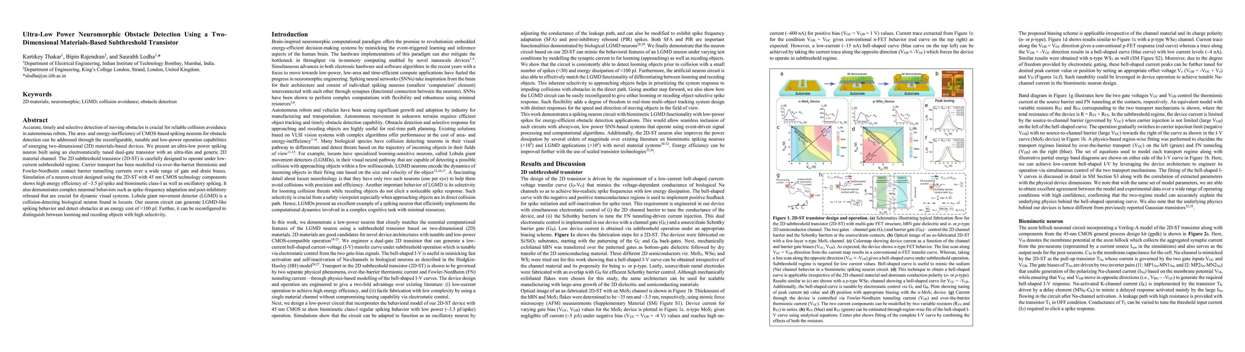
Accurate, timely and selective detection of moving obstacles is crucial for reliable collision avoidance in autonomous robots. The area- and energy-inefficiency of CMOS-based spiking neurons for obs...
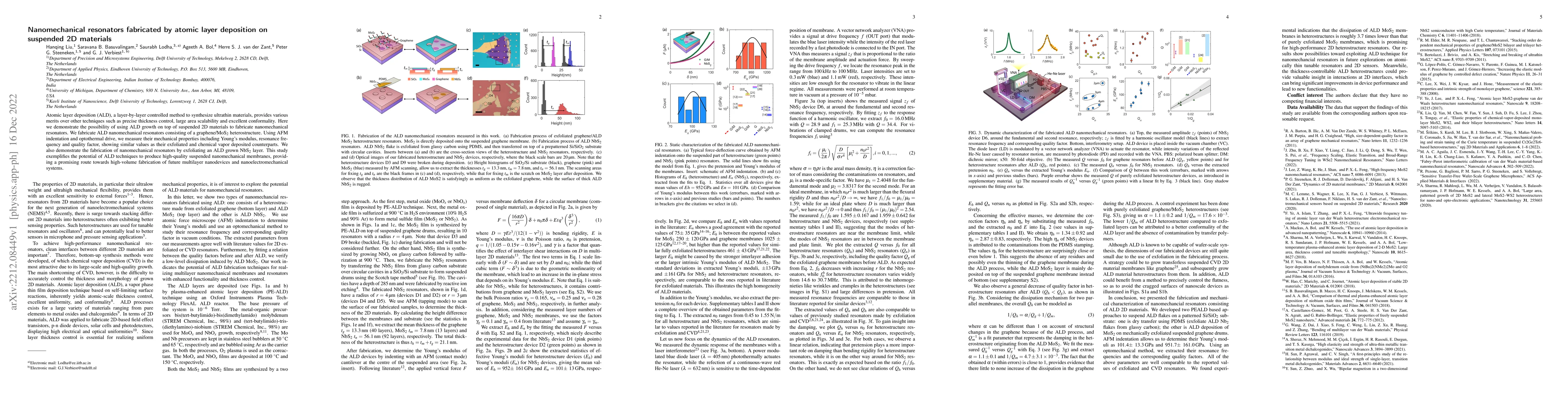
Atomic layer deposition (ALD), a layer-by-layer controlled method to synthesize ultrathin materials, provides various merits over other techniques such as precise thickness control, large area scala...
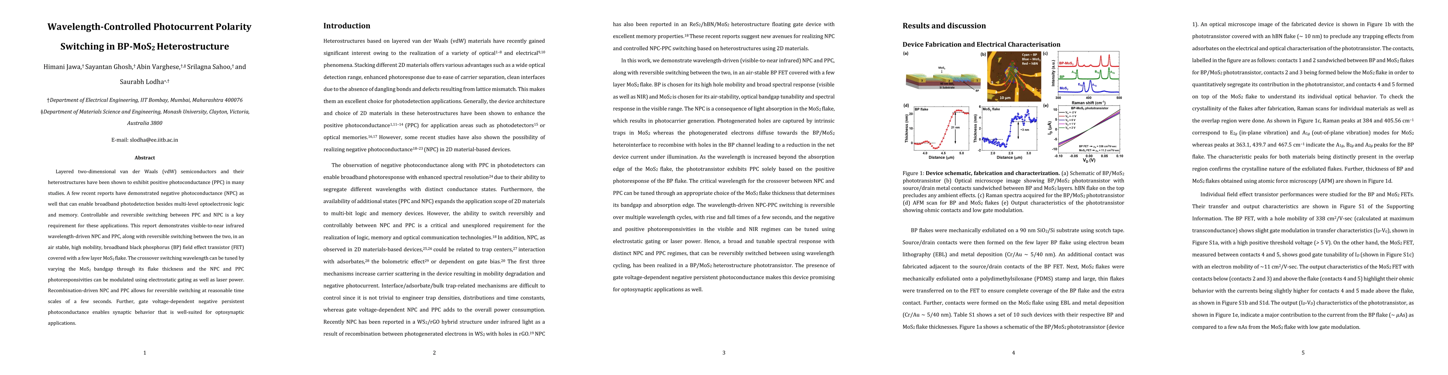
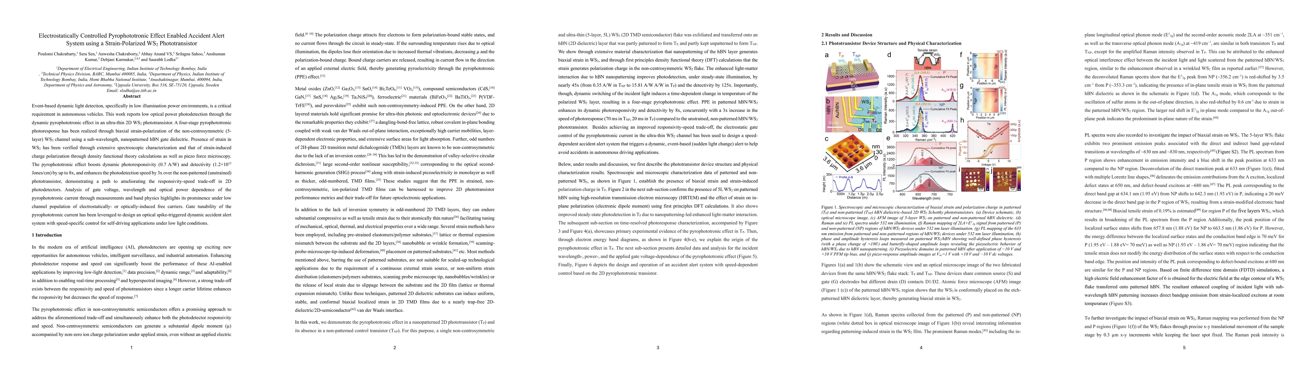
Layered two-dimensional van der Waals (vdW) semiconductors and their heterostructures have been shown to exhibit positive photoconductance (PPC) in many studies. A few recent reports have demonstrat...
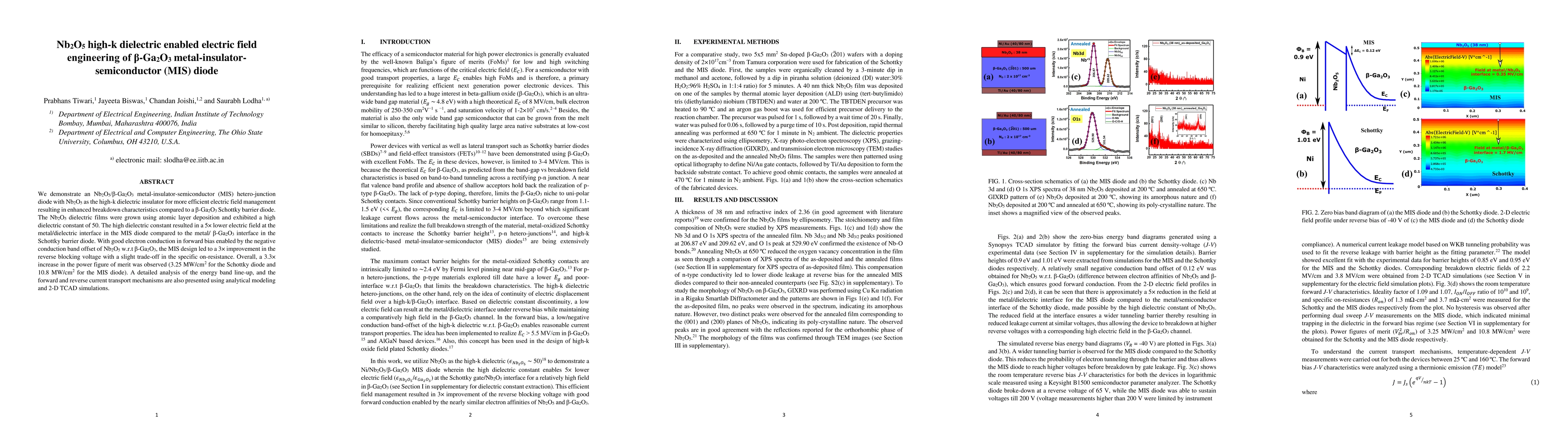
We demonstrate an Nb$_{2}$O$_{5}$/$\beta$-Ga$_{2}$O$_{3}$ metal-insulator-semiconductor (MIS) hetero-junction diode with Nb$_{2}$O$_{5}$ as the high-k dielectric insulator for more efficient electri...
The application of ultrathin two-dimensional (2D) perovskites in near-infrared and visible-range optoelectronics has been limited owing to their inherent wide bandgaps, large excitonic binding energ...
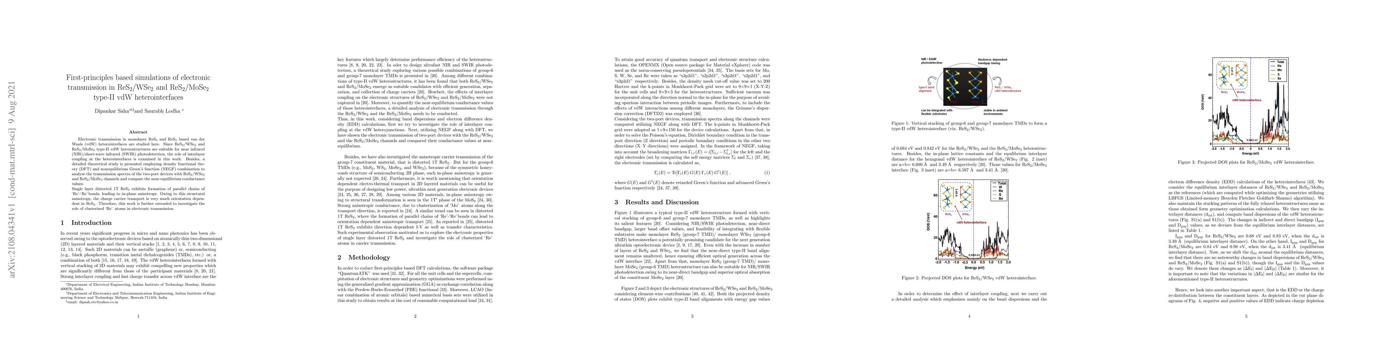
Electronic transmission in monolayer ReS$_{2}$ and ReS$_{2}$ based van der Waals (vdW) heterointerfaces are studied here. Since ReS$_{2}$/WSe$_{2}$ and ReS$_{2}$/MoSe$_{2}$ type-II vdW heterostructu...
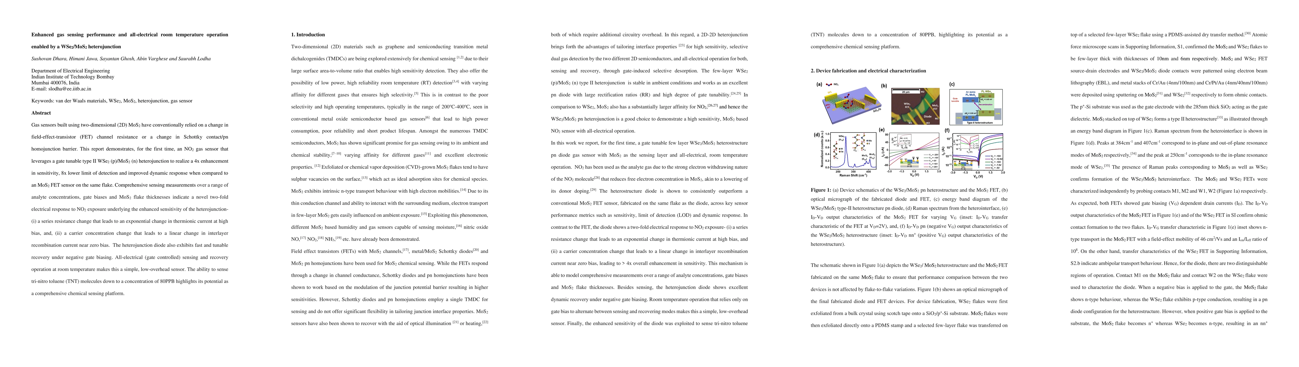
Gas sensors built using two-dimensional (2D) MoS2 have conventionally relied on a change in field-effect-transistor (FET) channel resistance or a change in Schottky contact/pn homojunction barrier. ...
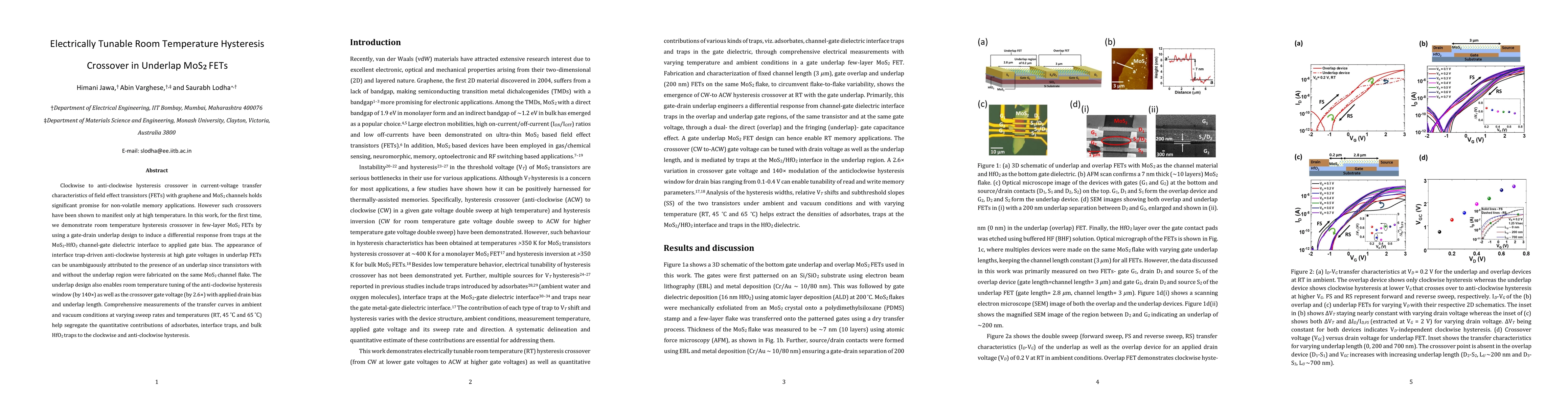
Clockwise to anti-clockwise hysteresis crossover in current-voltage transfer characteristics of field effect transistors (FETs) with graphene and MoS$_2$ channels holds significant promise for non-v...
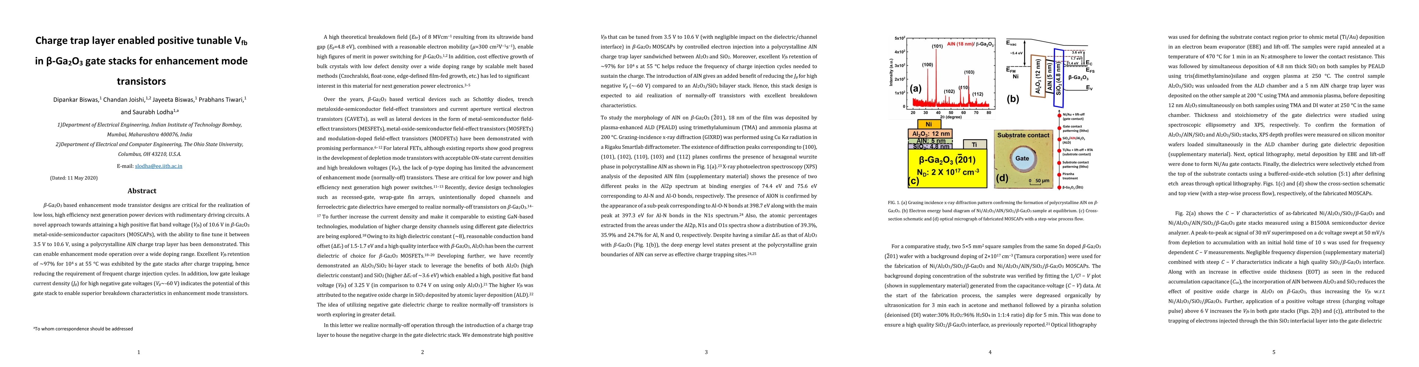
$\beta$-Ga$_{2}$O$_{3}$ based enhancement mode transistor designs are critical for the realization of low loss, high efficiency next generation power devices with rudimentary driving circuits. A nov...
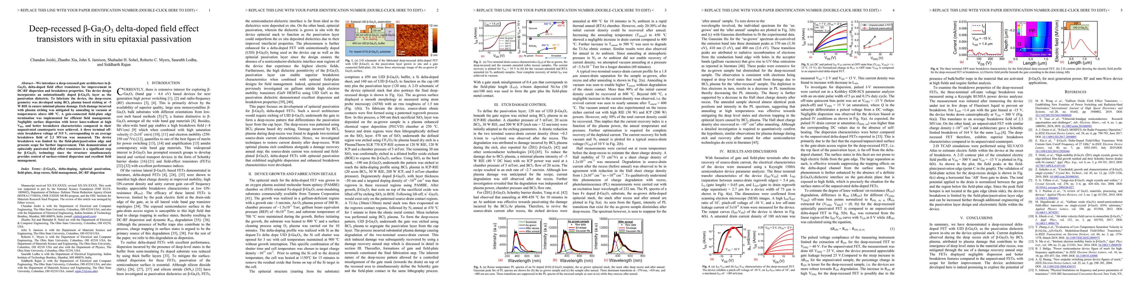
We introduce a deep-recessed gate architecture in $\beta$-Ga$_2$O$_3$ delta-doped field effect transistors for improvement in DC-RF dispersion and breakdown properties. The device design incorporate...
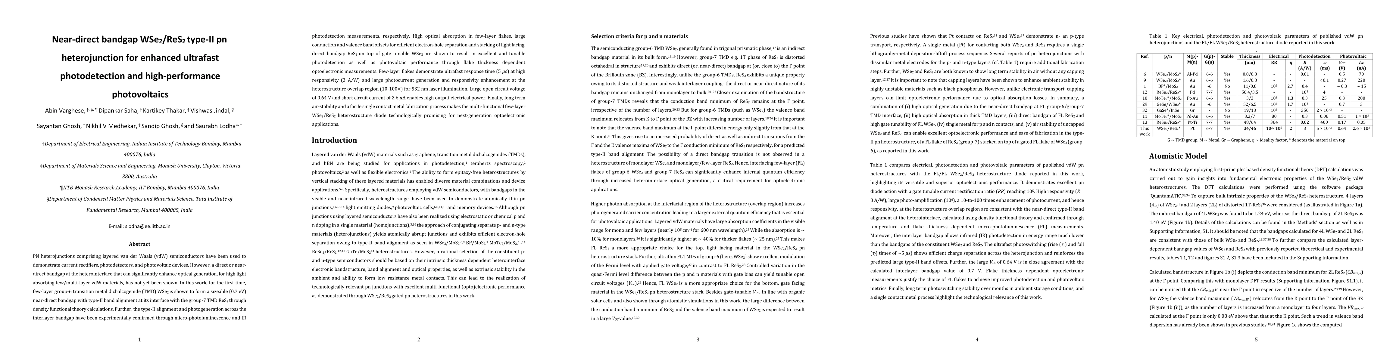
PN heterojunctions comprising layered van der Waals (vdW) semiconductors have been used to demonstrate current rectifiers, photodetectors, and photovoltaic devices. However, a direct or near-direct ...
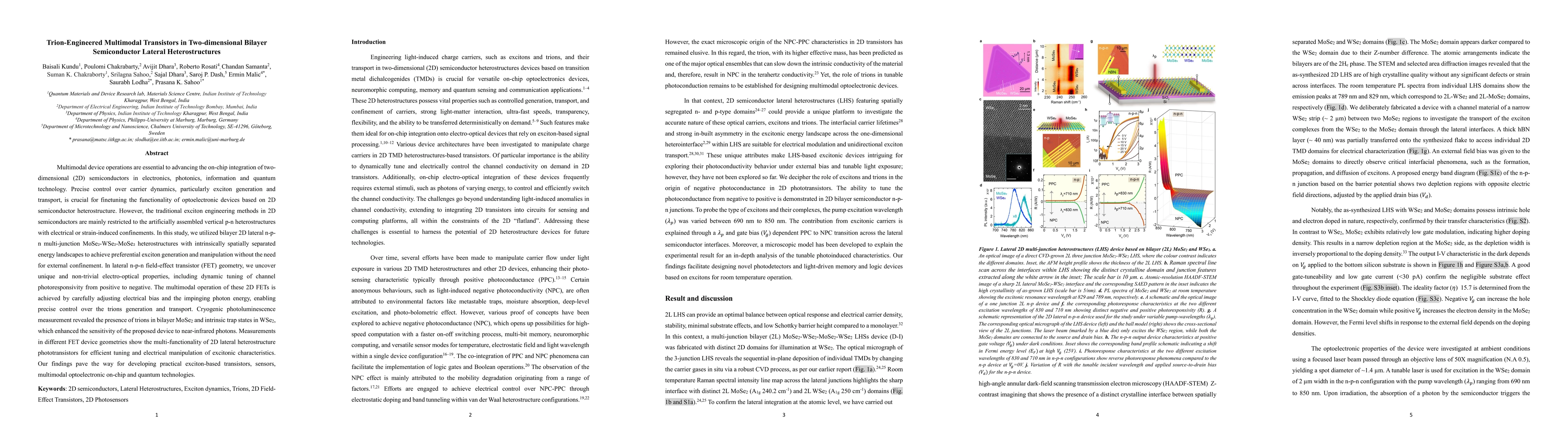
Multimodal device operations are essential to advancing the integration of 2D semiconductors in electronics, photonics, information and quantum technology. Precise control over carrier dynamics, parti...
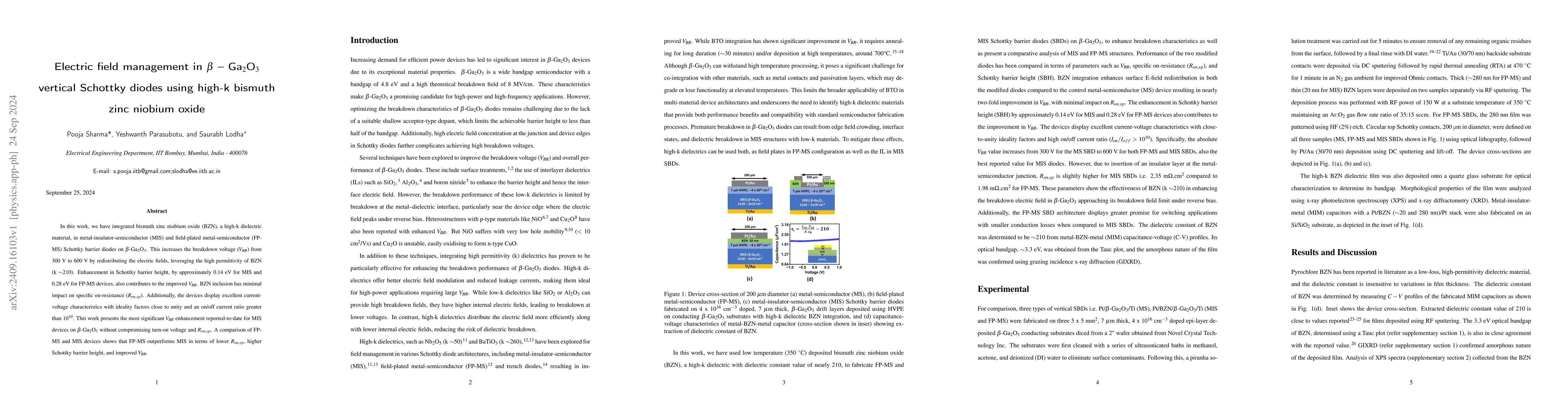
In this work, we have integrated bismuth zinc niobium oxide (BZN), a high-k dielectric material, in metal-insulator-semiconductor (MIS) and field-plated metal-semiconductor (FP-MS) Schottky barrier di...
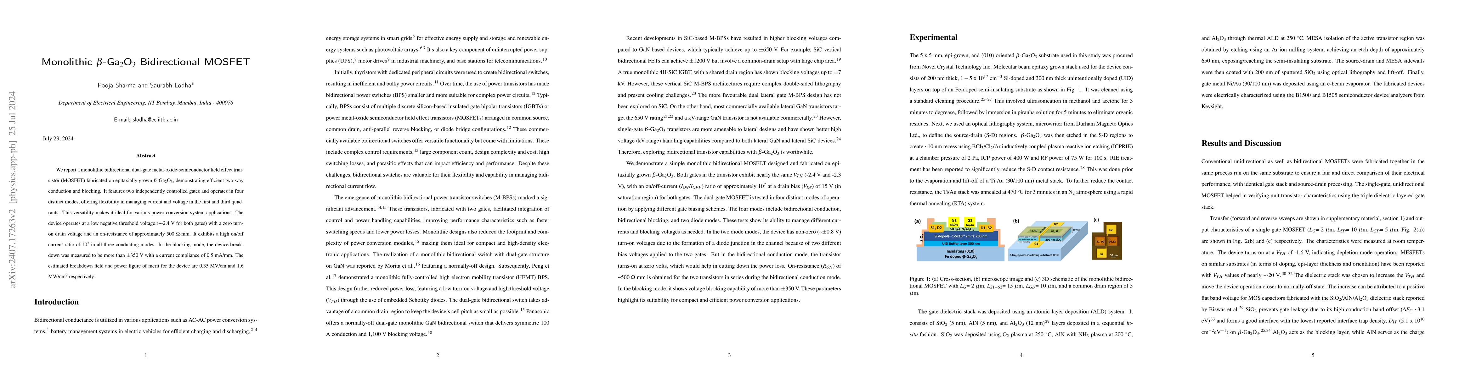
We report a monolithic bidirectional dual-gate metal-oxide-semiconductor field effect transistor (MOSFET) fabricated on epitaxially grown beta-Ga2O3, demonstrating efficient two-way conduction and blo...
Neuromorphic in-memory computing requires area-efficient architecture for seamless and low latency parallel processing of large volumes of data. Here, we report a compact, vertically integrated/strati...
Event-based dynamic light detection, specifically in low illumination power environments, is a critical requirement in autonomous vehicles. This work reports low optical power photodetection through t...
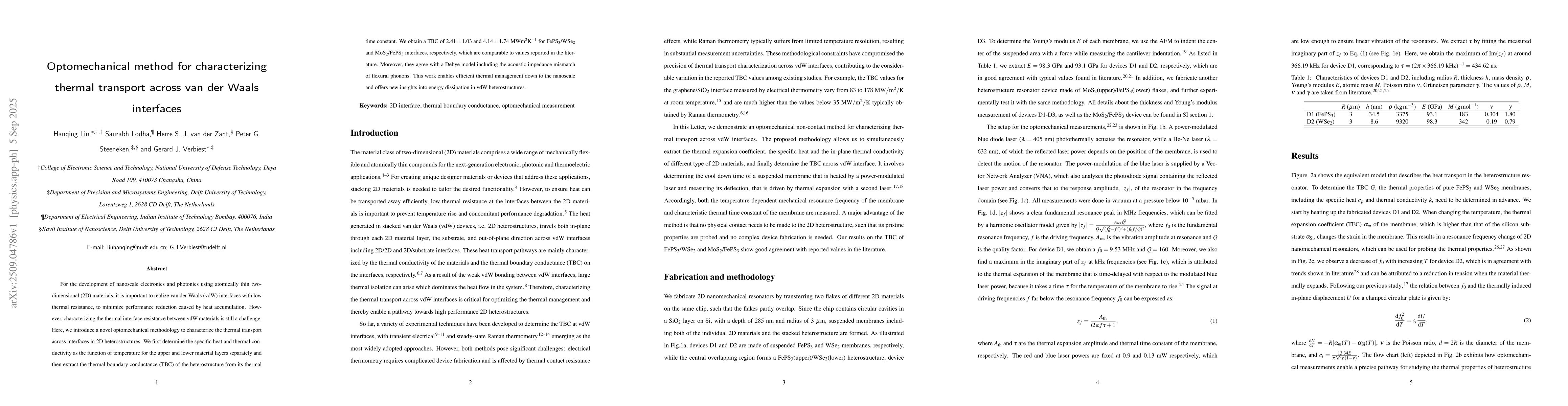
For the development of nanoscale electronics and photonics using atomically thin two-dimensional (2D) materials, it is important to realize van der Waals (vdW) interfaces with low thermal resistance, ...
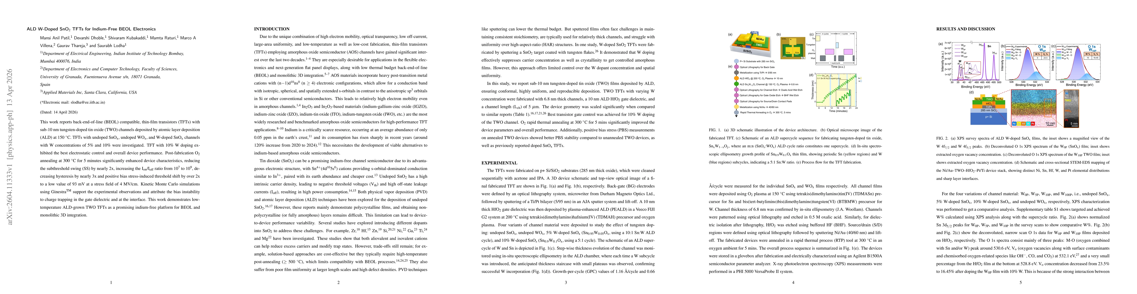
This work reports back-end-of-line (BEOL) compatible, thin-film transistors (TFTs) with sub-10 nm tungsten-doped tin oxide (TWO) channels deposited by atomic layer deposition (ALD) at 150 $^\circ$C. T...
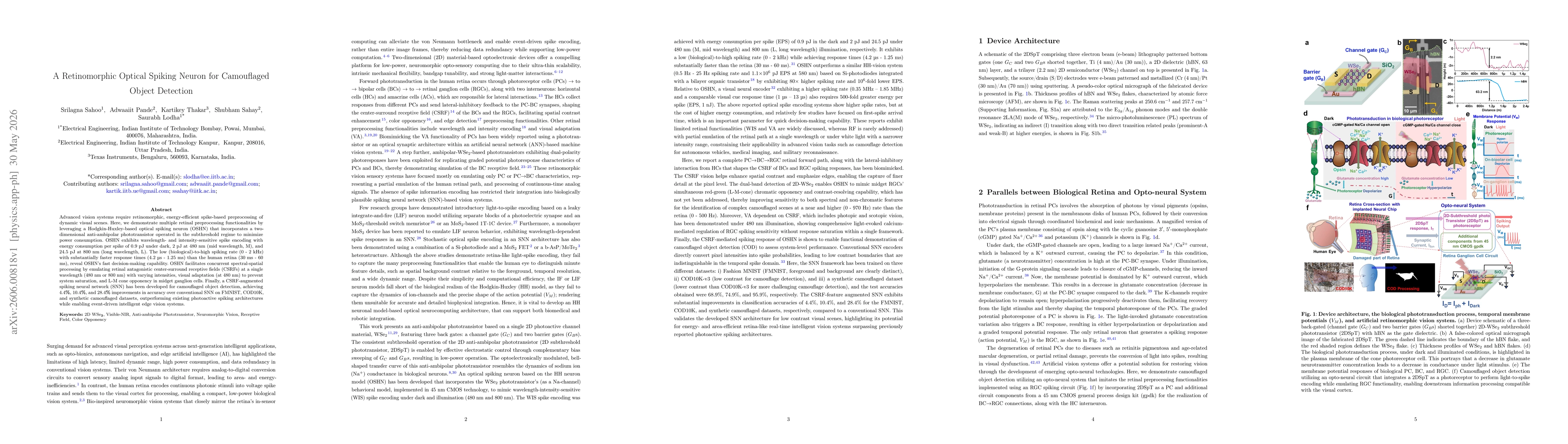
Advanced vision systems require retinomorphic, energy-efficient spike-based preprocessing of dynamic visual scenes. Here, we demonstrate multiple retinal preprocessing functionalities by leveraging a ...