Academic Profile
Statistics
Similar Authors
Papers on arXiv
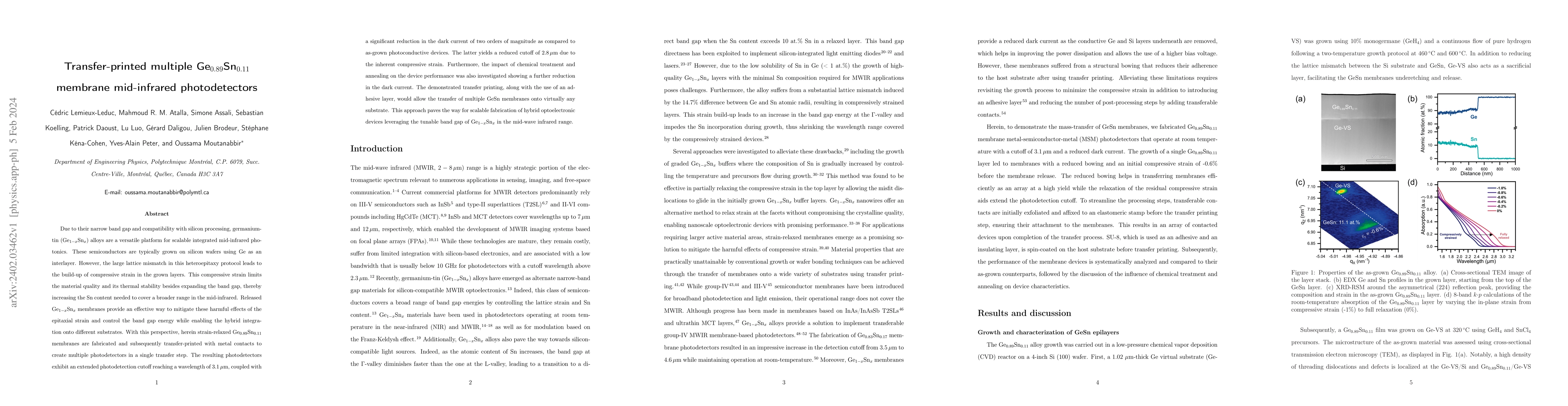
Due to their narrow band gap and compatibility with silicon processing, germanium-tin (Ge$_{1-x}$Sn$_x$) alloys are a versatile platform for scalable integrated mid-infrared photonics. These semicon...
There is an increasing need for silicon-compatible high bandwidth extended-short wave infrared (e-SWIR) photodetectors (PDs) to implement cost-effective and scalable optoelectronic devices. These sy...
Achieving high crystalline quality Ge$_{1-x}$Sn$_{x}$ semiconductors at Sn content exceeding 10\% is quintessential to implementing the long sought-after silicon-compatible mid-infrared photonics. H...
Cost-effective mid-wave infrared (MWIR) optoelectronic devices are of utmost importance to a plethora of applications such as night vision, thermal sensing, autonomous vehicles, free-space communica...
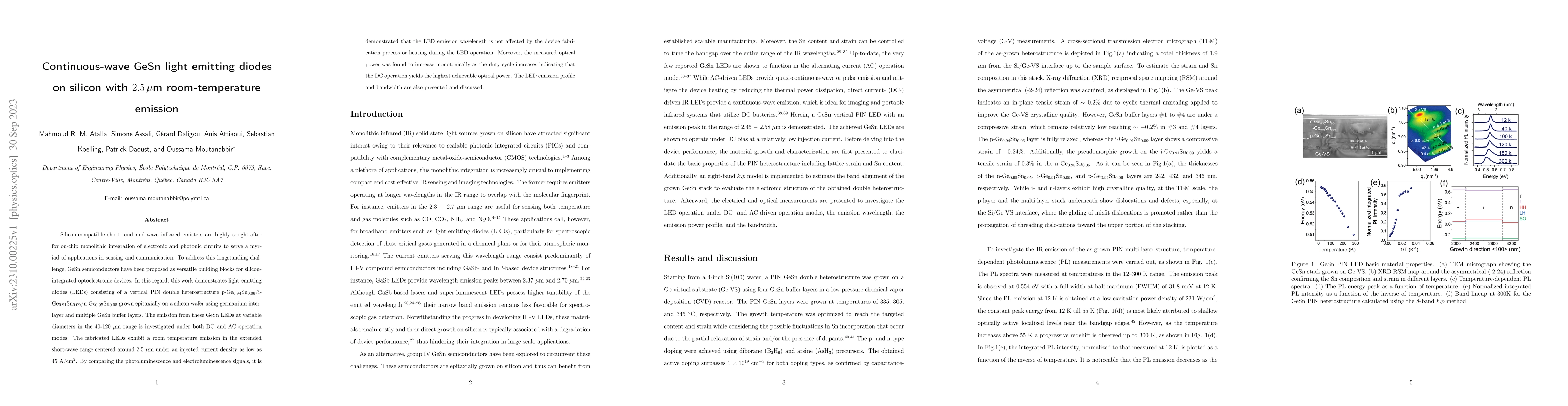
Silicon-compatible short- and mid-wave infrared emitters are highly sought-after for on-chip monolithic integration of electronic and photonic circuits to serve a myriad of applications in sensing a...
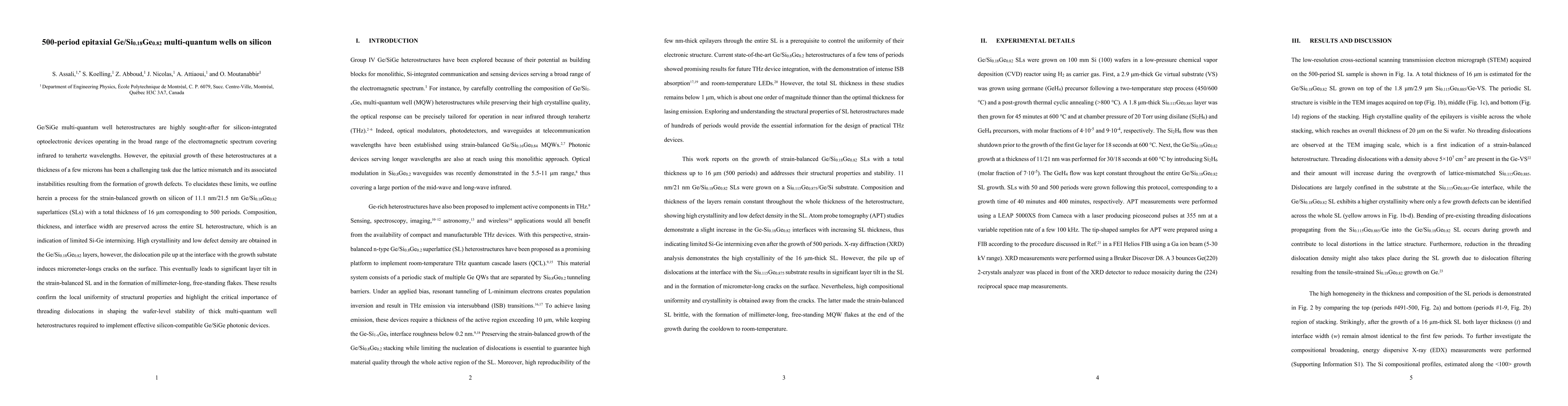
Ge/SiGe multi-quantum well heterostructures are highly sought-after for silicon-integrated optoelectronic devices operating in the broad range of the electromagnetic spectrum covering infrared to te...
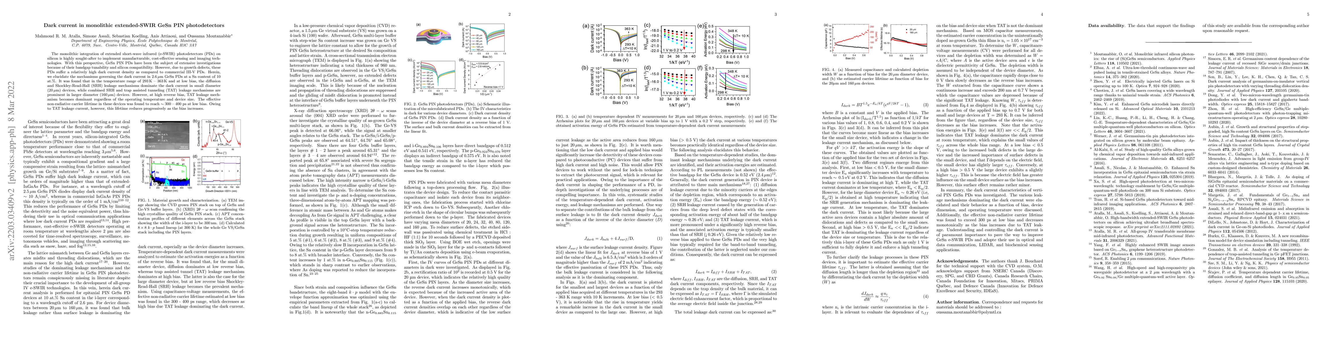
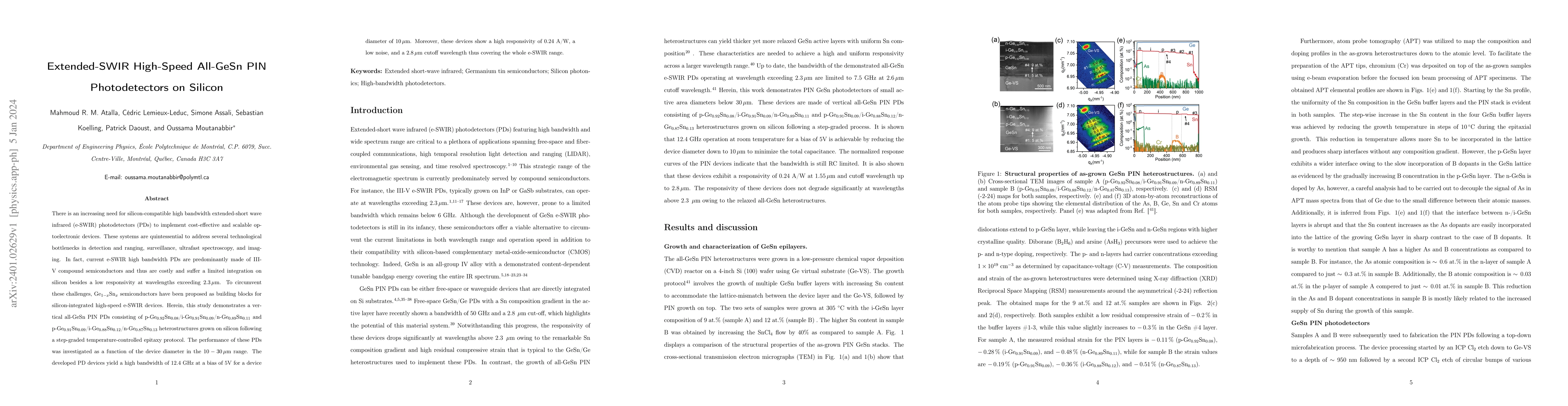
The monolithic integration of extended short-wave infrared (e-SWIR) photodetectors (PDs) on silicon is highly sought-after to implement manufacturable, cost-effective sensing and imaging technologie...
Electron spins in Si/SiGe quantum wells suffer from nearly degenerate conduction band valleys, which compete with the spin degree of freedom in the formation of qubits. Despite attempts to enhance t...
The prospect of GeSn semiconductors for silicon-integrated infrared optoelectronics brings new challenges related to the metastability of this class of materials. As a matter of fact, maintaining a ...
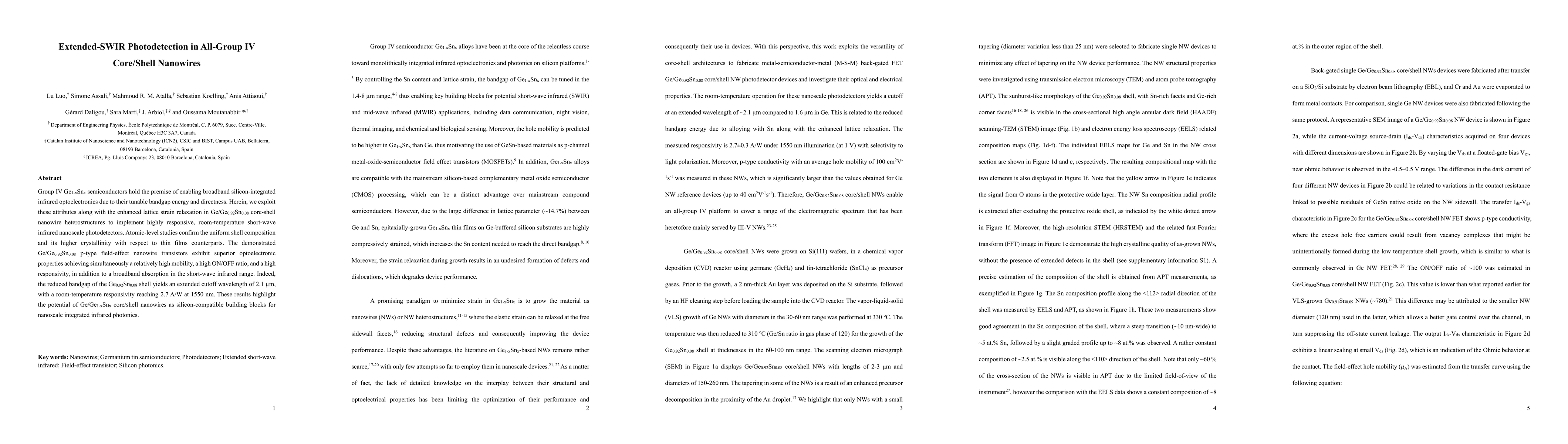
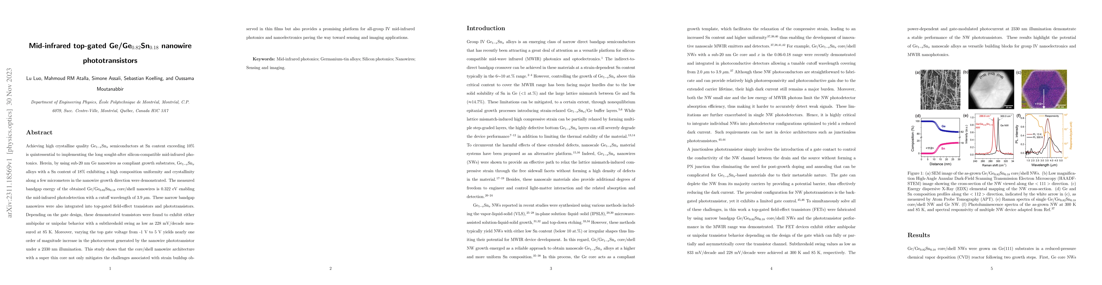
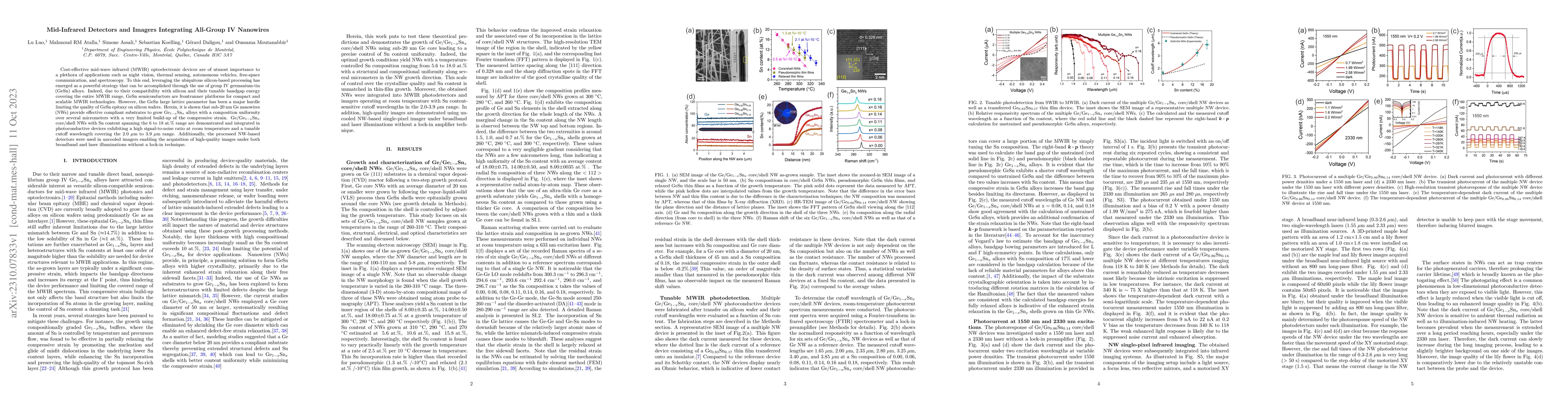
Group IV Ge1-xSnx semiconductors hold the premise of enabling broadband silicon-integrated infrared optoelectronics due to their tunable bandgap energy and directness. Herein, we exploit these attri...
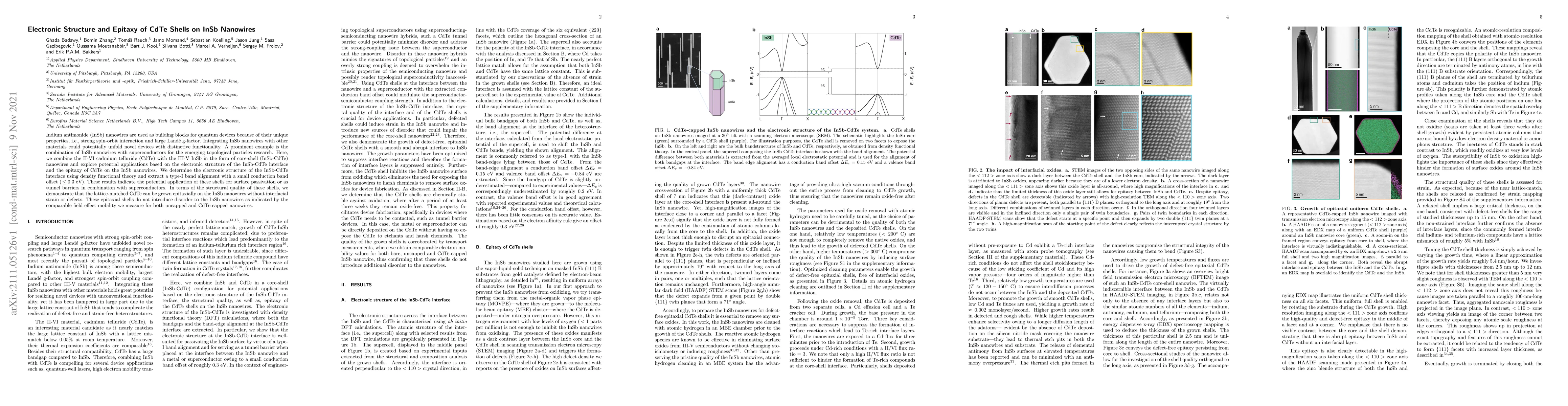
Indium antimonide (InSb) nanowires are used as building blocks for quantum devices because of their unique properties, i.e., strong spin-orbit interaction and large Land\'e g-factor. Integrating InS...
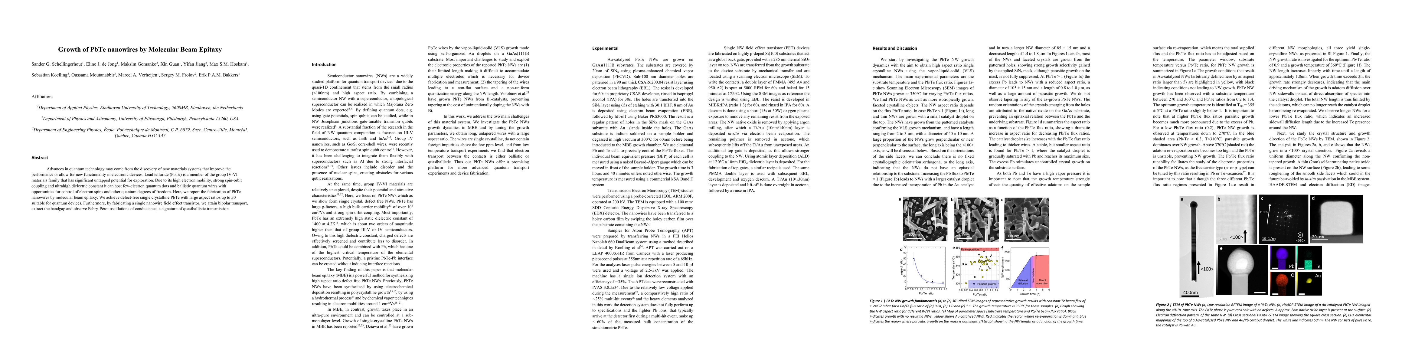
Advances in quantum technology may come from the discovery of new materials systems that improve the performance or allow for new functionality in electronic devices. Lead telluride (PbTe) is a memb...
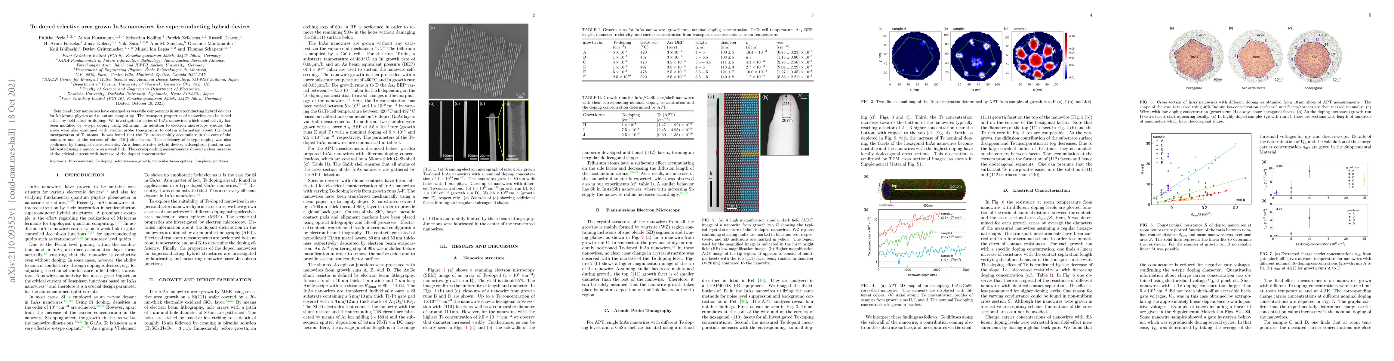
Semiconductor nanowires have emerged as versatile components in superconducting hybrid devices for Majorana physics and quantum computing. The transport properties of nanowires can be tuned either b...
Strong spin-orbit semiconductor nanowires coupled to a superconductor are predicted to host Majorana zero modes. Exchange (braiding) operations of Majorana modes form the logical gates of a topologi...
A true monolithic infrared photonics platform is within reach if strain and bandgap energy can be independently engineered in SiGeSn semiconductors. Herein, we investigate the structural and optoele...
We report electron transport studies on InSb-Al hybrid semiconductor-superconductor nanowire devices. Tunnelling spectroscopy is used to measure the evolution of subgap states while varying magnetic...
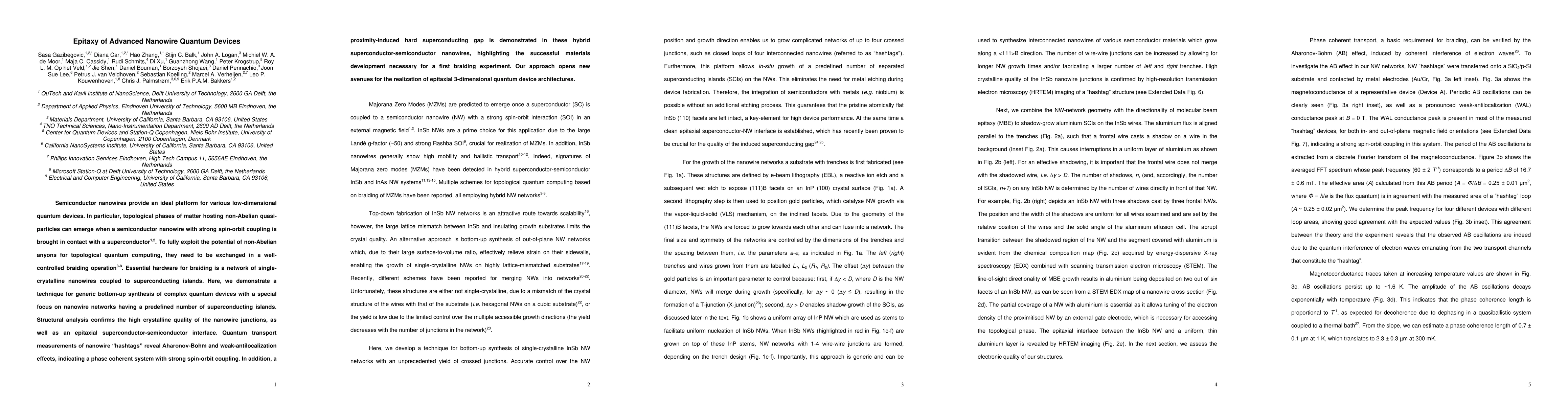
Semiconductor nanowires provide an ideal platform for various low-dimensional quantum devices. In particular, topological phases of matter hosting non-Abelian quasi-particles can emerge when a semic...
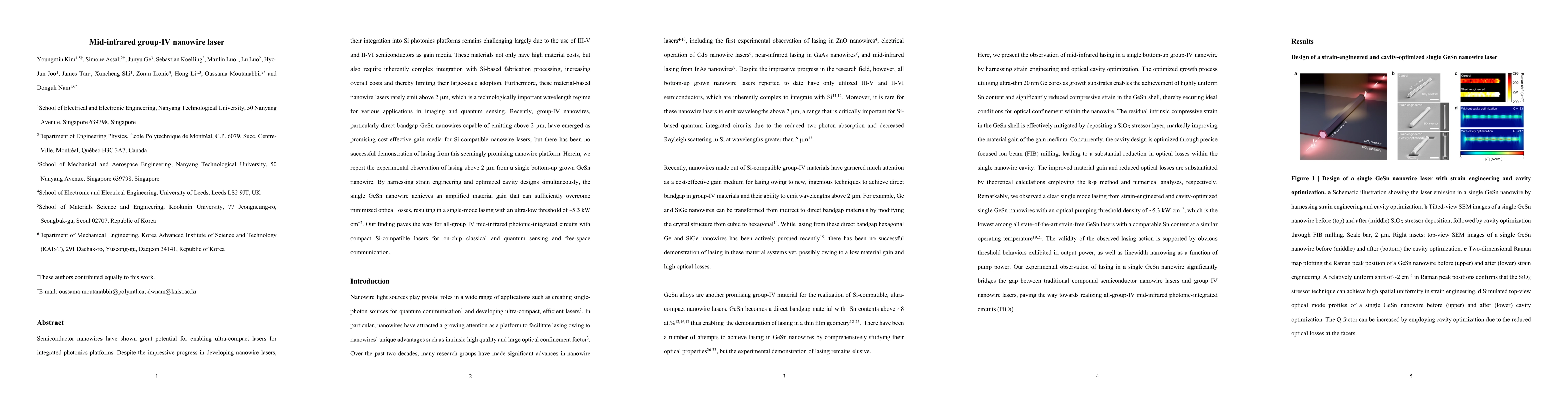
Semiconductor nanowires have shown great potential for enabling ultra-compact lasers for integrated photonics platforms. Despite the impressive progress in developing nanowire lasers, their integratio...
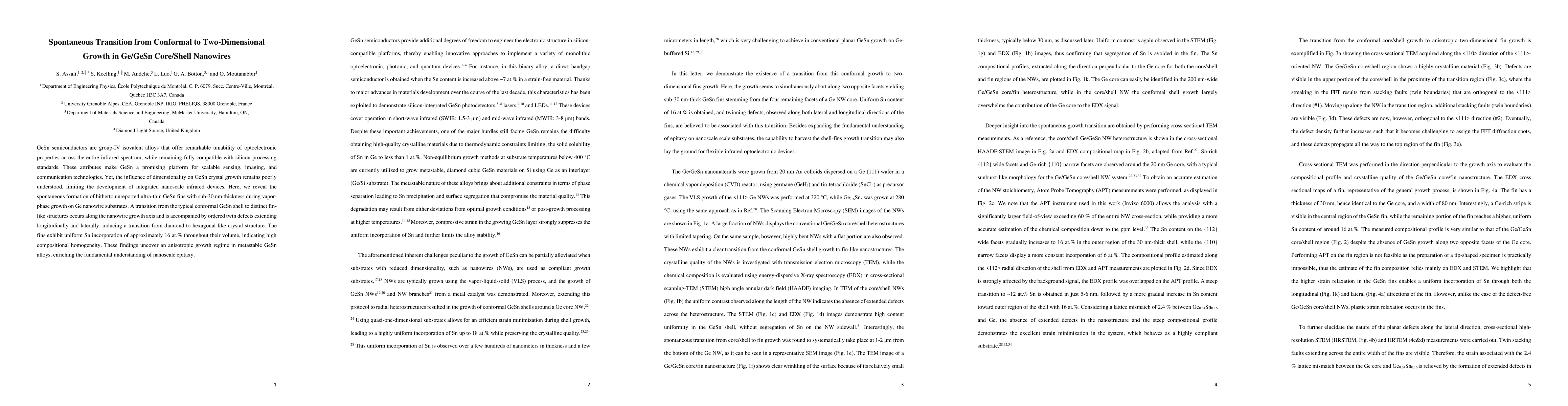
GeSn semiconductors are group-IV isovalent alloys that offer remarkable tunability of optoelectronic properties across the entire infrared spectrum, while remaining fully compatible with silicon proce...
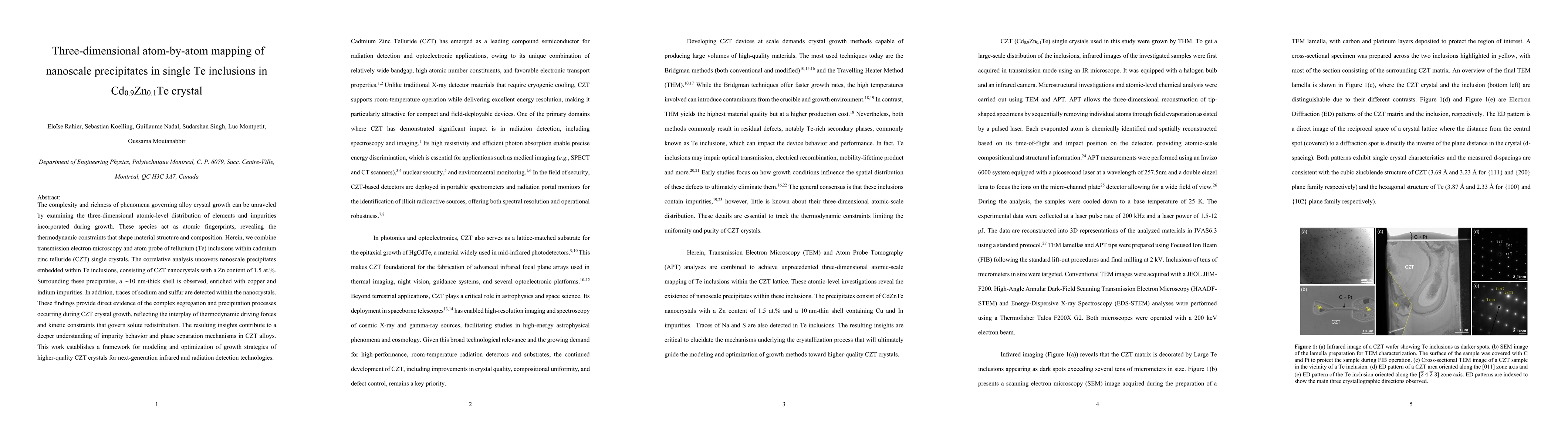
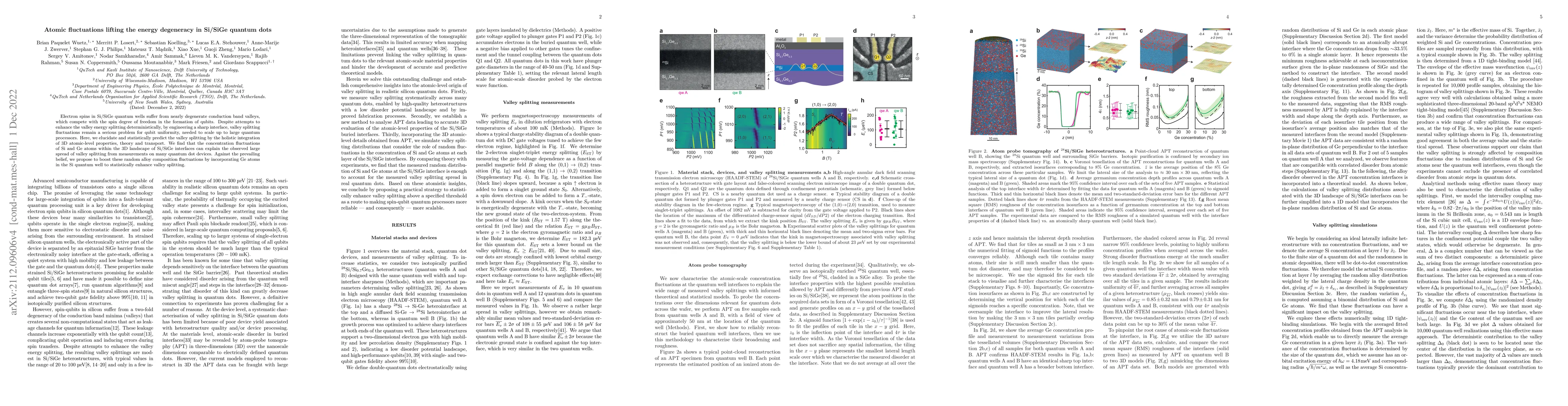
The complexity and richness of phenomena governing alloy crystal growth can be unraveled by examining the three-dimensional atomic-level distribution of elements and impurities incorporated during gro...
Germanium quantum well heterostructures have rapidly emerged as a leading platform for solid-state quantum information processing; however, material quality limits scalability, and higher structural q...