Academic Profile
Statistics
Similar Authors
Papers on arXiv
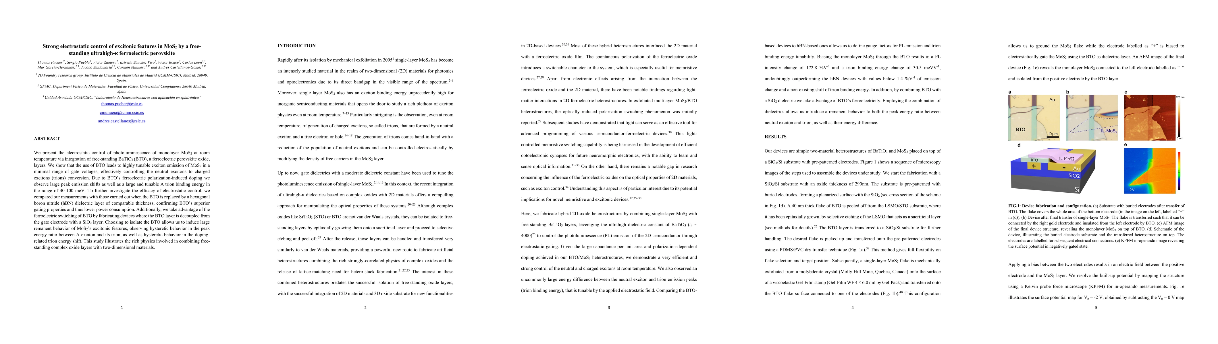
We present the electrostatic control of photoluminescence of monolayer MoS$_2$ at room temperature via integration of free-standing BaTiO$_3$ (BTO), a ferroelectric perovskite oxide, layers. We show...
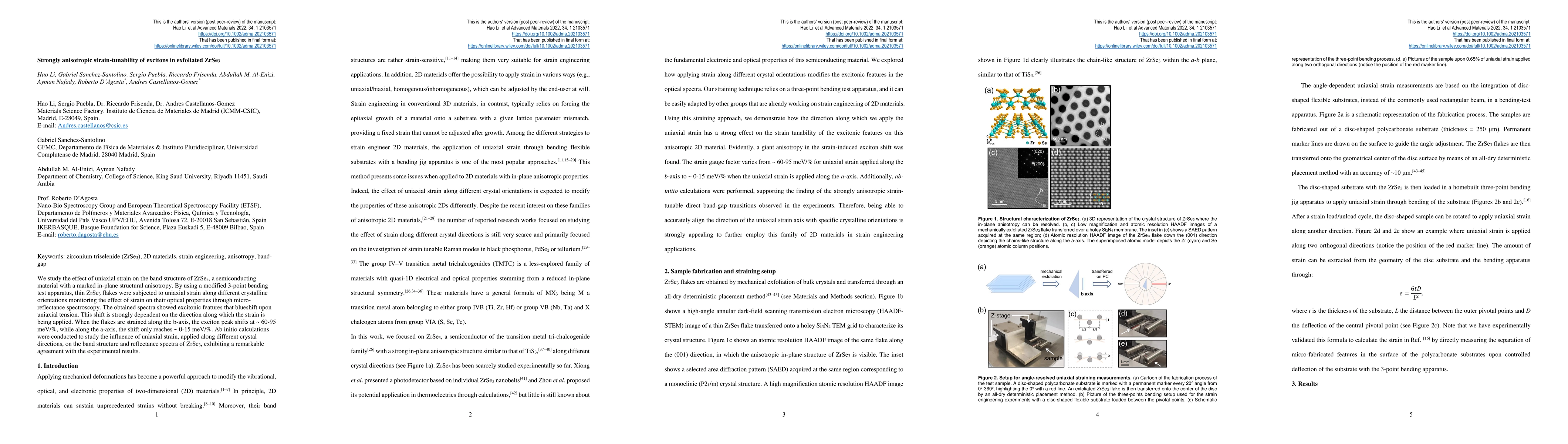
We study the effect of uniaxial strain on the band structure of ZrSe$_3$, a semiconducting material with a marked in-plane structural anisotropy. By using a modified 3-point bending test apparatus, ...
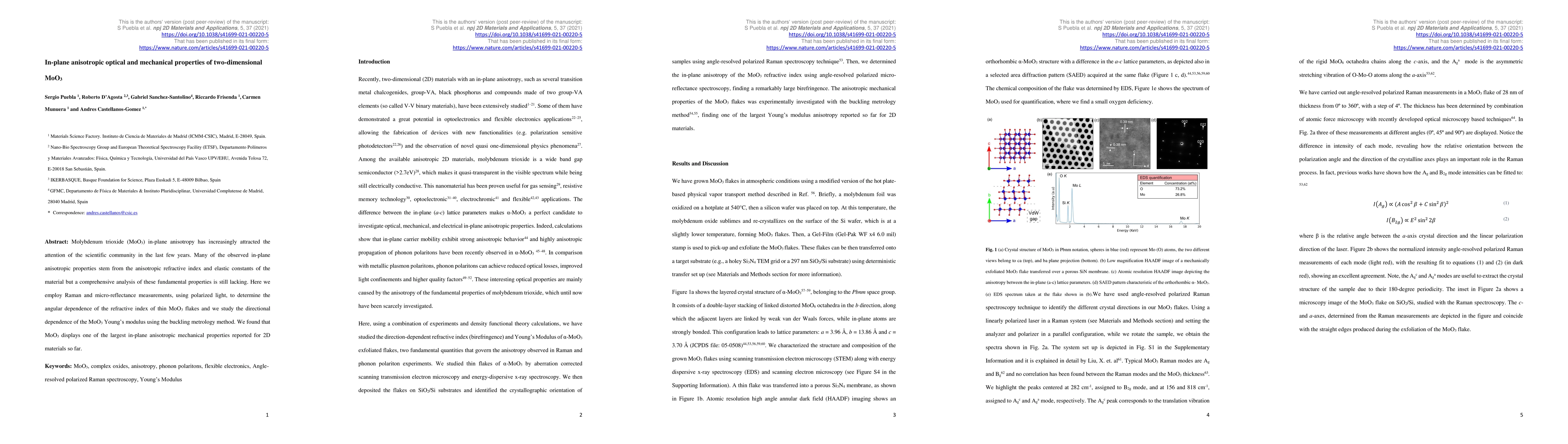
Molybdenum trioxide (MoO$_3$) in-plane anisotropy has increasingly attracted the attention of the scientific community in the last few years. Many of the observed in-plane anisotropic properties ste...
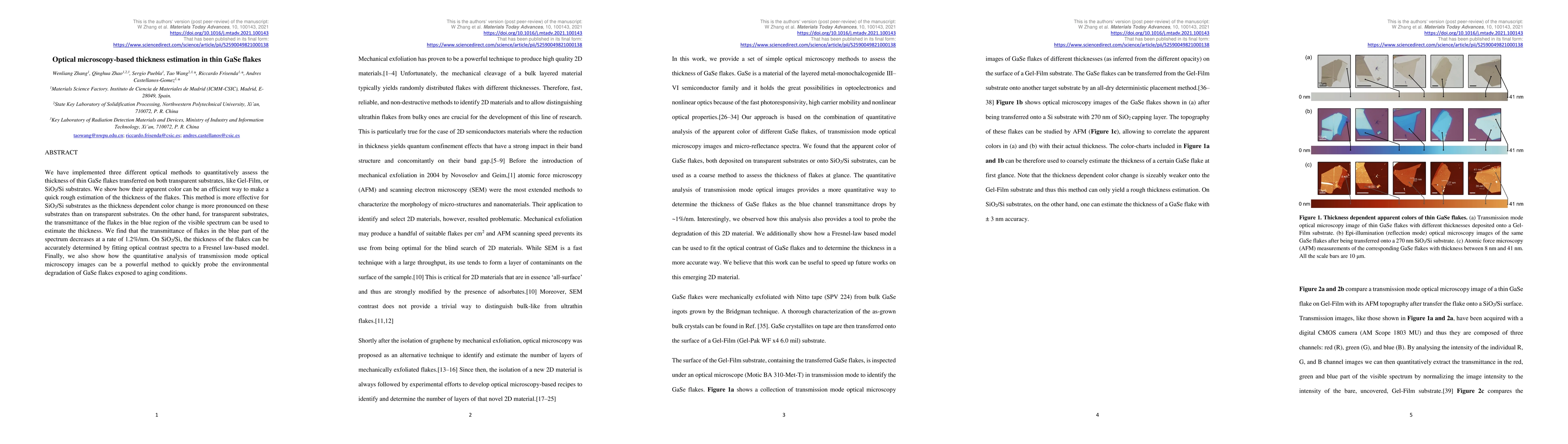
We have implemented three different optical methods to quantitatively assess the thickness of thin GaSe flakes transferred on both transparent substrates, like Gel-Film, or SiO2/Si substrates. We sh...
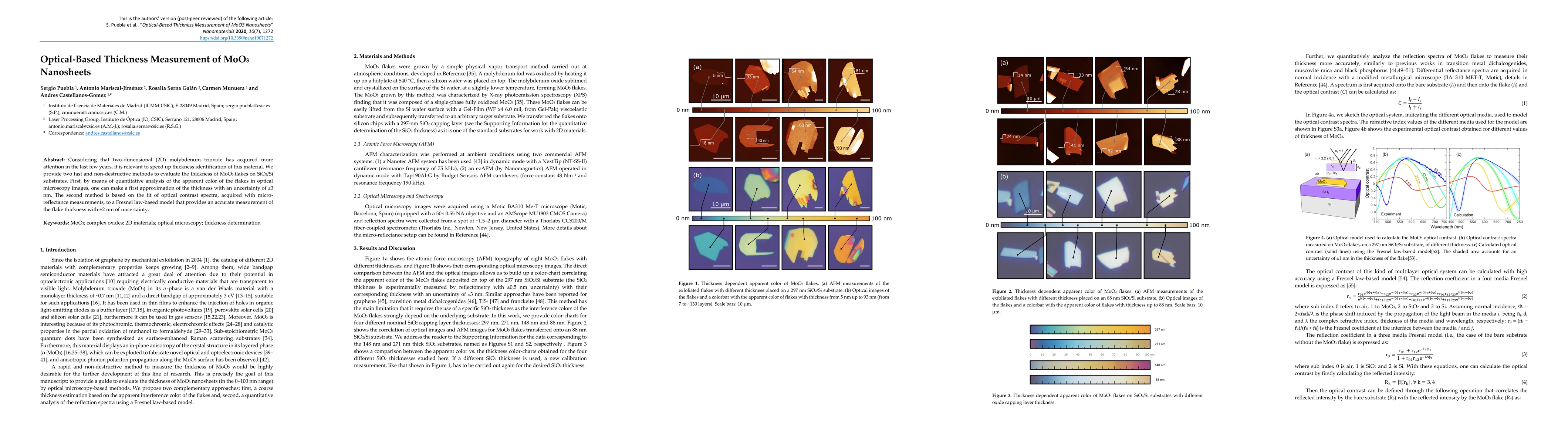
Considering that two-dimensional (2D) molybdenum trioxide has acquired more attention in the last few years, it is relevant to speed up thickness identification of this material. We provide two fast...
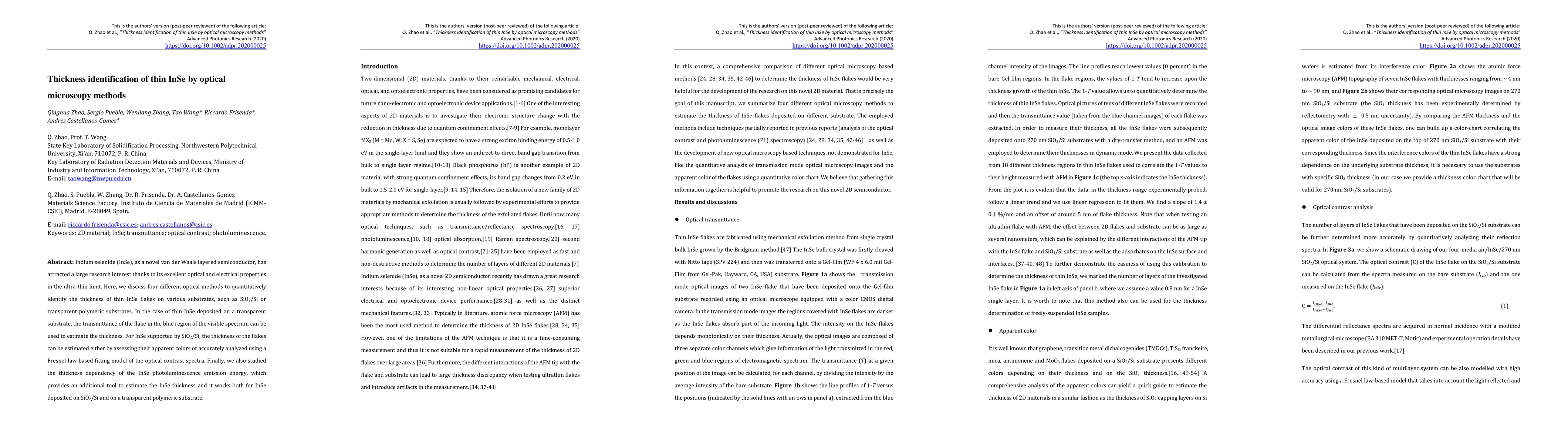
Indium selenide (InSe), as a novel van der Waals layered semiconductor, has attracted a large research interest thanks to its excellent optical and electrical properties in the ultra-thin limit. Her...