Academic Profile
Statistics
Similar Authors
Papers on arXiv
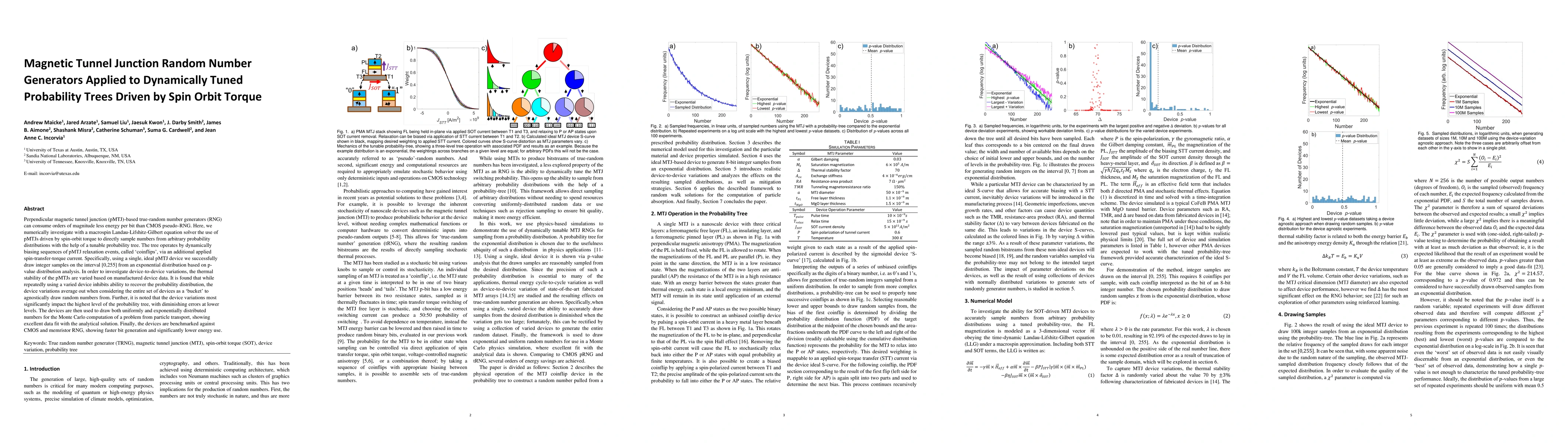
Perpendicular magnetic tunnel junction (pMTJ)-based true-random number generators (RNG) can consume orders of magnitude less energy per bit than CMOS pseudo-RNG. Here, we numerically investigate wit...
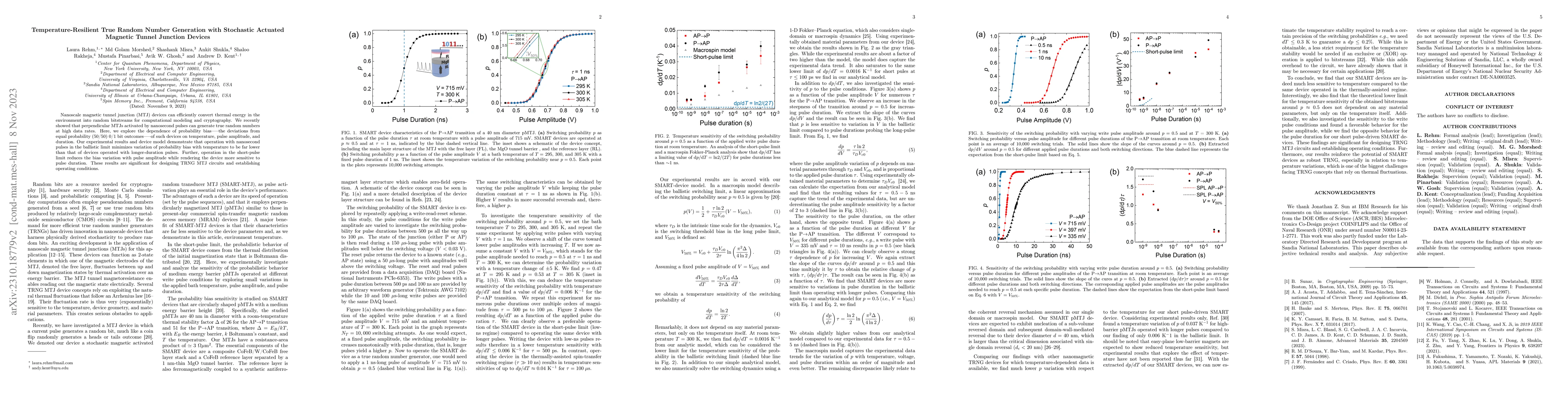
Nanoscale magnetic tunnel junction (MTJ) devices can efficiently convert thermal energy in the environment into random bitstreams for computational modeling and cryptography. We recently showed that...
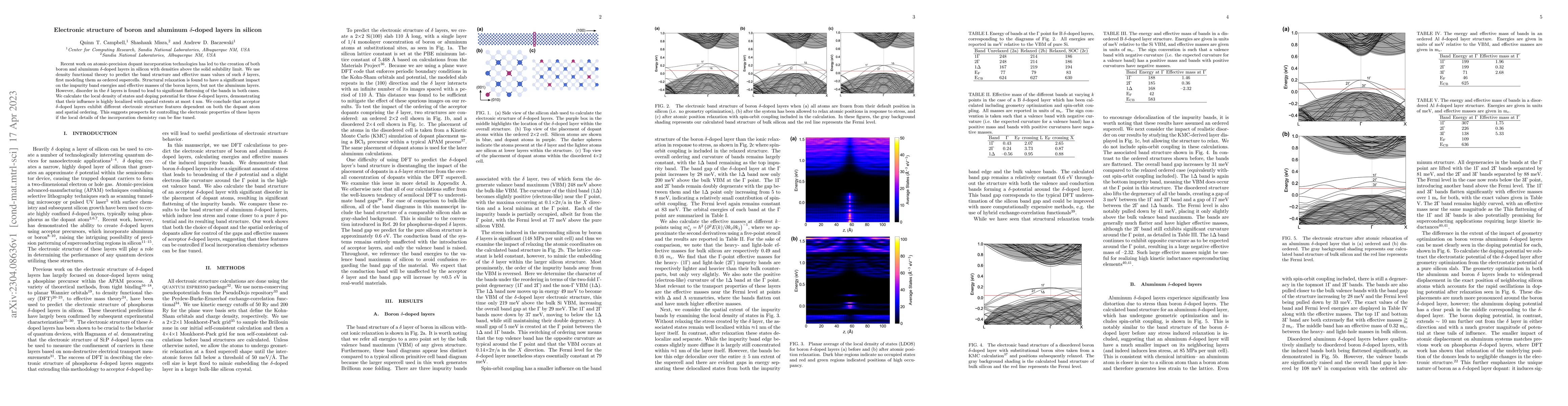
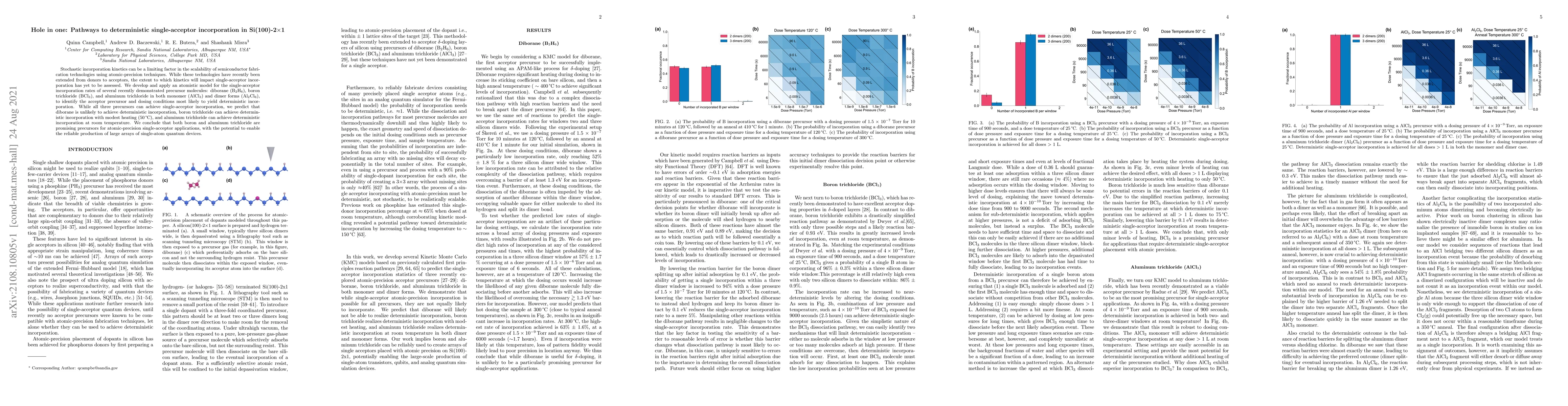
Recent work on atomic-precision dopant incorporation technologies has led to the creation of both boron and aluminum $\delta$-doped layers in silicon with densities above the solid solubility limit....
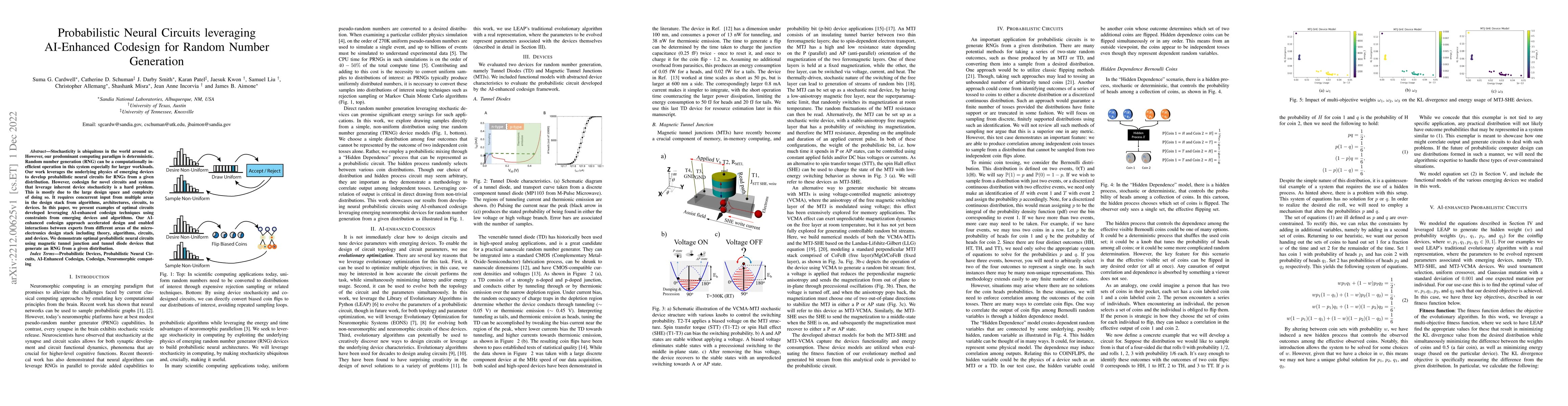
Stochasticity is ubiquitous in the world around us. However, our predominant computing paradigm is deterministic. Random number generation (RNG) can be a computationally inefficient operation in thi...
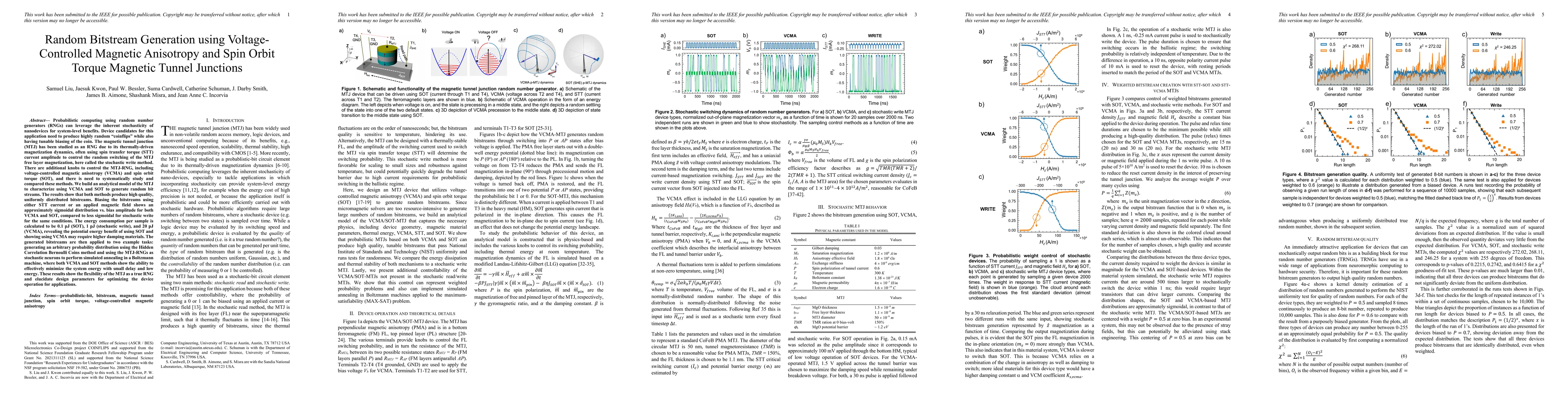
Probabilistic computing using random number generators (RNGs) can leverage the inherent stochasticity of nanodevices for system-level benefits. The magnetic tunnel junction (MTJ) has been studied as...
The classical Drude model provides an accurate description of the plasma resonance of three-dimensional materials, but only partially explains two-dimensional systems where quantum mechanical effect...
The recently-developed ability to control phosphorous-doping of silicon at an atomic level using scanning tunneling microscopy (STM), a technique known as atomic-precision-advanced-manufacturing (AP...
Atomic-precision advanced manufacturing enables the placement of dopant atoms within $\pm$1 lattice site in crystalline Si. However, it has recently been shown that reaction kinetics can introduce u...
BCl$_3$ is a promising candidate for atomic-precision acceptor doping in Si, but optimizing the electrical properties of structures created with this technique requires a detailed understanding of a...
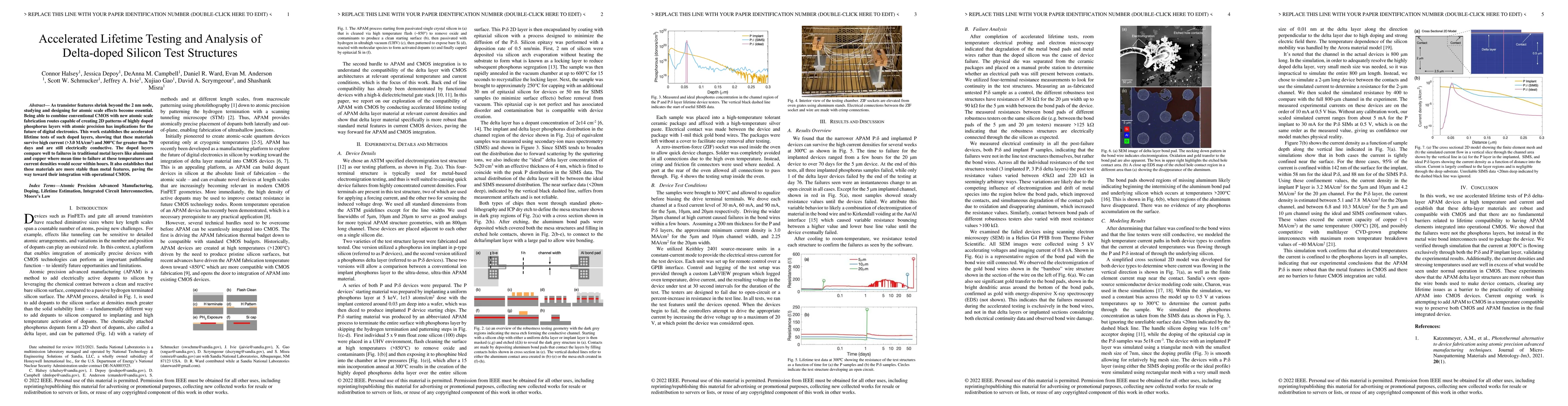
As transistor features shrink beyond the 2 nm node, studying and designing for atomic scale effects become essential. Being able to combine conventional CMOS with new atomic scale fabrication routes...
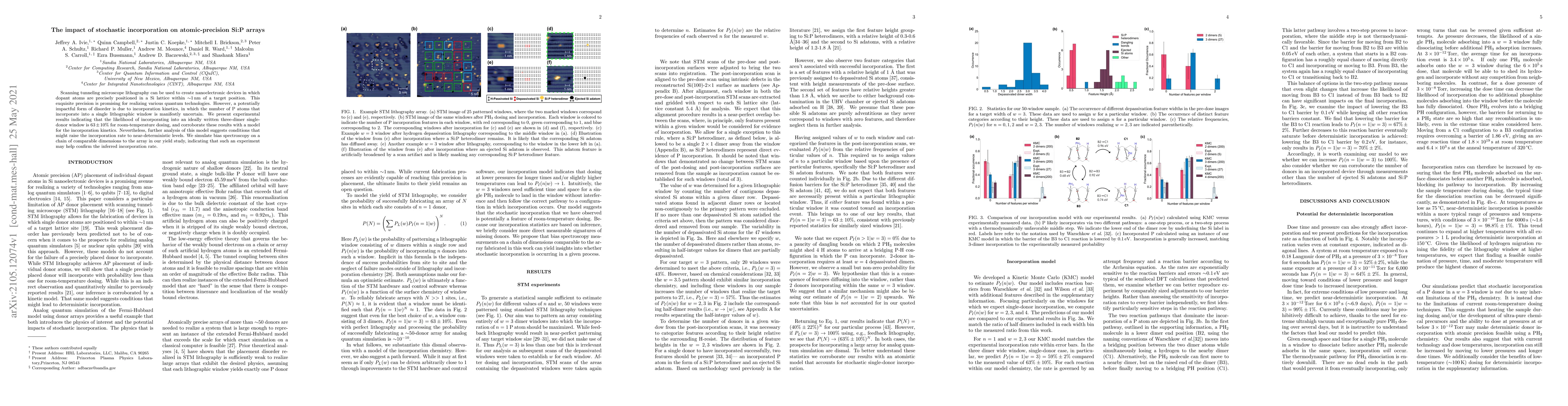
Stochastic incorporation kinetics can be a limiting factor in the scalability of semiconductor fabrication technologies using atomic-precision techniques. While these technologies have recently been...
Scanning tunneling microscope lithography can be used to create nanoelectronic devices in which dopant atoms are precisely positioned in a Si lattice within $\sim$1 nm of a target position. This exq...
The adsorption of AlCl$_{3}$ on Si(100) and the effect of annealing the AlCl$_{3}$-dosed substrate was studied to reveal key surface processes for the development of atomic-precision acceptor-doping...
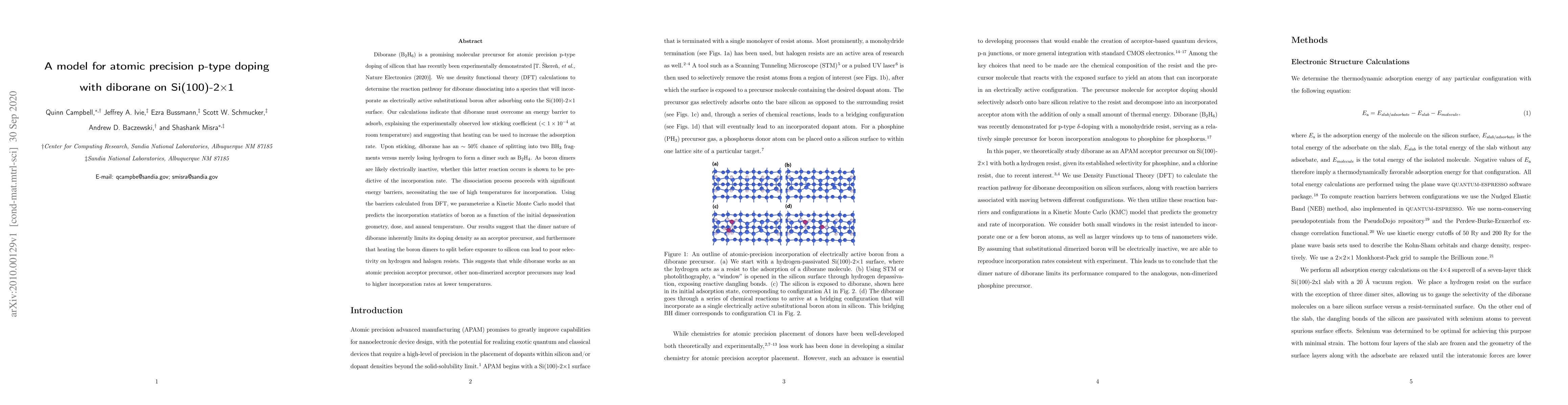
Diborane (B$_2$H$_6$) is a promising molecular precursor for atomic precision p-type doping of silicon that has recently been experimentally demonstrated [T. {\v{S}}kere{\v{n}}, \textit{et al.,} Nat...
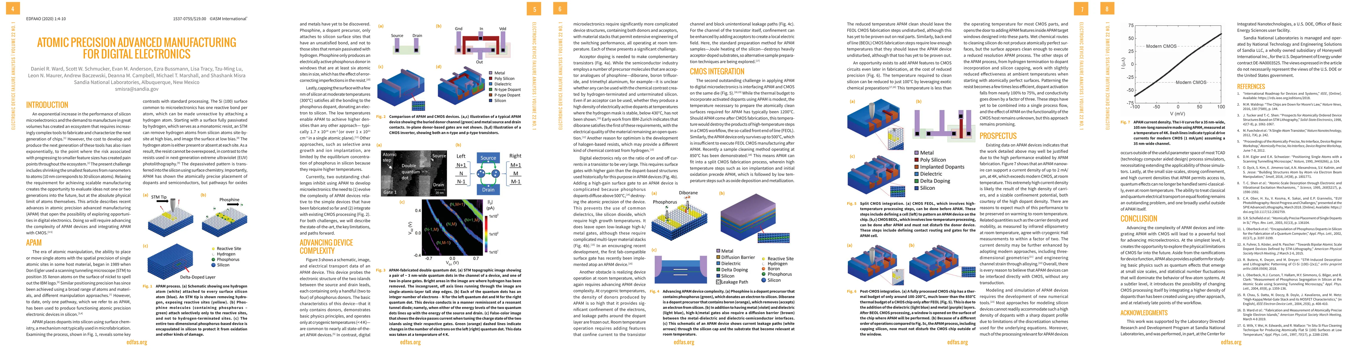
An exponential increase in the performance of silicon microelectronics and the demand to manufacture in great volumes has created an ecosystem that requires increasingly complex tools to fabricate a...
Quantum simulators are a promising technology on the spectrum of quantum devices from specialized quantum experiments to universal quantum computers. These quantum devices utilize entanglement and m...
Spin states in semiconductors provide exceptionally stable and noise-resistant environments for qubits, positioning them as optimal candidates for reliable quantum computing technologies. The proposal...
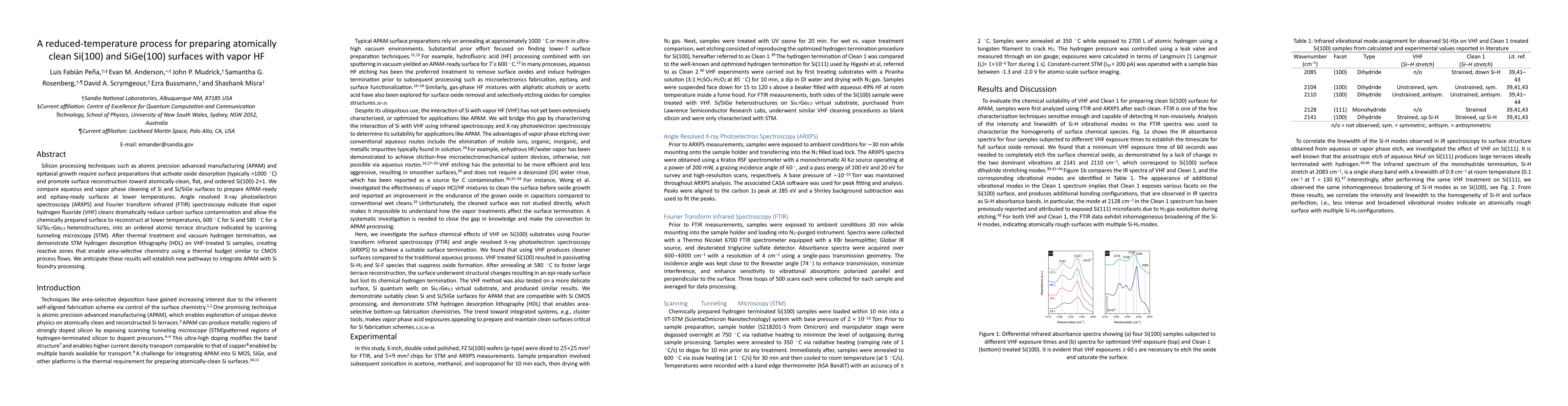
Silicon processing techniques such as atomic precision advanced manufacturing (APAM) and epitaxial growth require surface preparations that activate oxide desorption (typically >1000 $^{\circ}$C) and ...
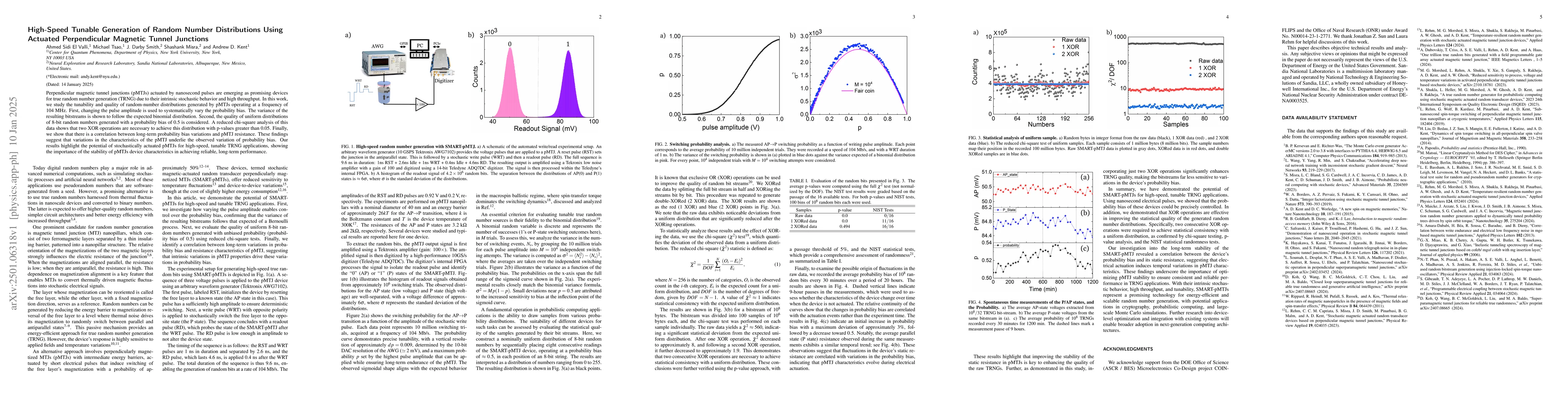
Perpendicular magnetic tunnel junctions (pMTJs) actuated by nanosecond pulses are emerging as promising devices for true random number generation (TRNG) due to their intrinsic stochastic behavior and ...
One of the most promising acceptor precursors for atomic-precision $\delta$-doping of silicon is BCl$_3$. The chemical pathway, and the resulting kinetics, through which BCl$_3$ adsorbs and dissociate...
Silicon can be heavily doped with phosphorus in a single atomic layer (a $\delta$ layer), significantly altering the electronic structure of the conduction bands within the material. Recent progress h...