Academic Profile
Statistics
Similar Authors
Papers on arXiv
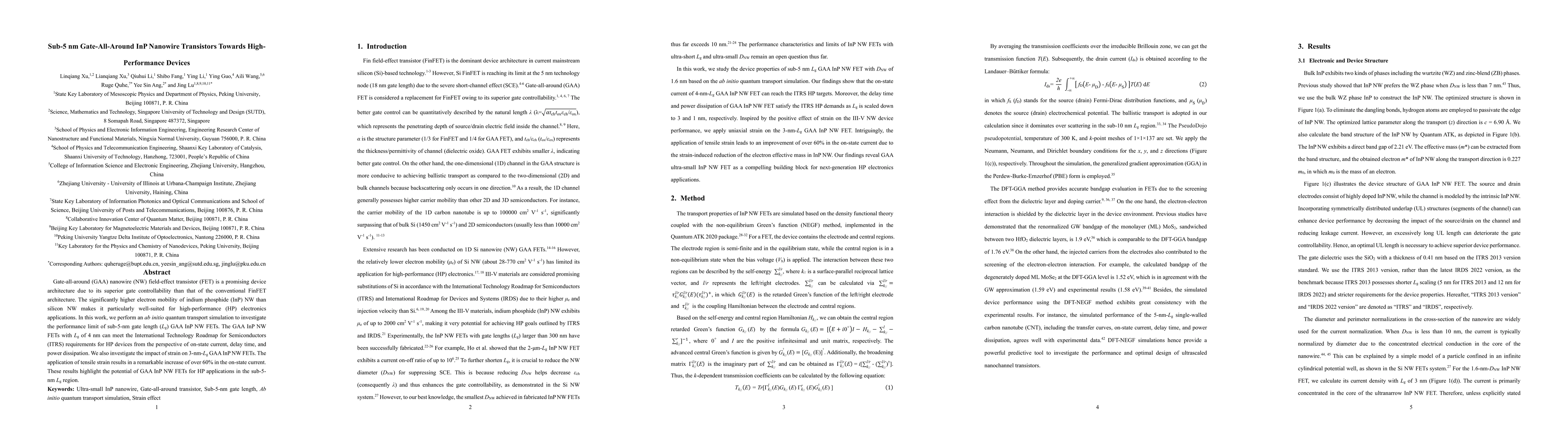
Gate-all-around (GAA) nanowire (NW) field-effect transistor (FET) is a promising device architecture due to its superior gate controllability than that of the conventional FinFET architecture. The s...
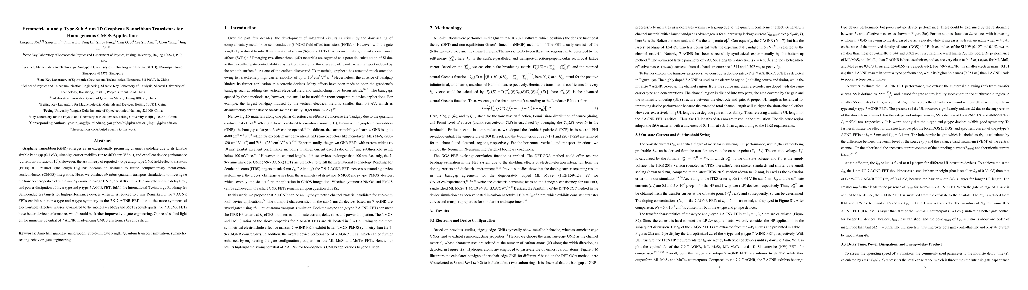
Graphene nanoribbon (GNR) emerges as an exceptionally promising channel candidate due to its tunable sizable bandgap (0-3 eV), ultrahigh carrier mobility (up to 4600 cm^(2) V^(-1) s^(-1)), and excelle...
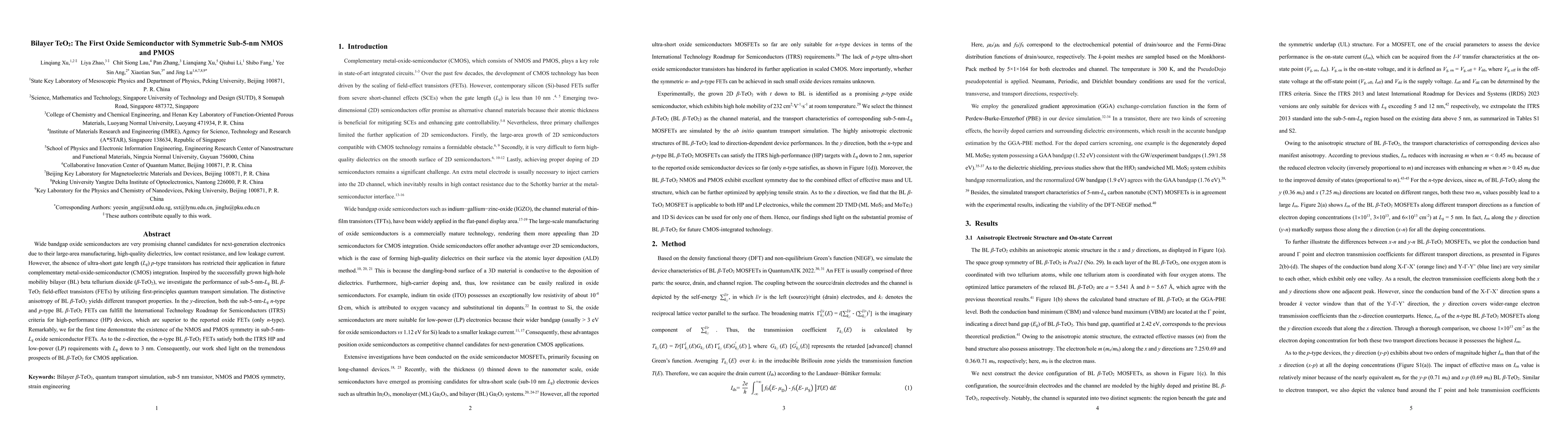
Wide bandgap oxide semiconductors are very promising channel candidates for next-generation electronics due to their large-area manufacturing, high-quality dielectrics, low contact resistance, and low...
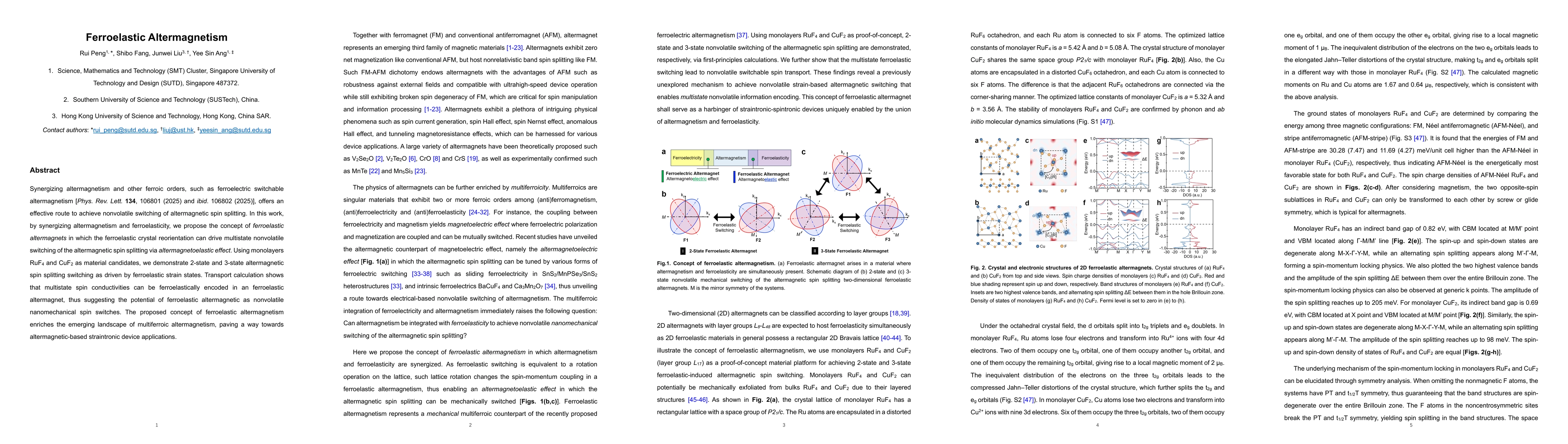
Synergizing altermagnetism and other ferroic orders, such as ferroelectric switchable altermagnetism [Phys. Rev. Lett. 134, 106801 (2025) and ibid. 106802 (2025)], offers an effective route to achieve...
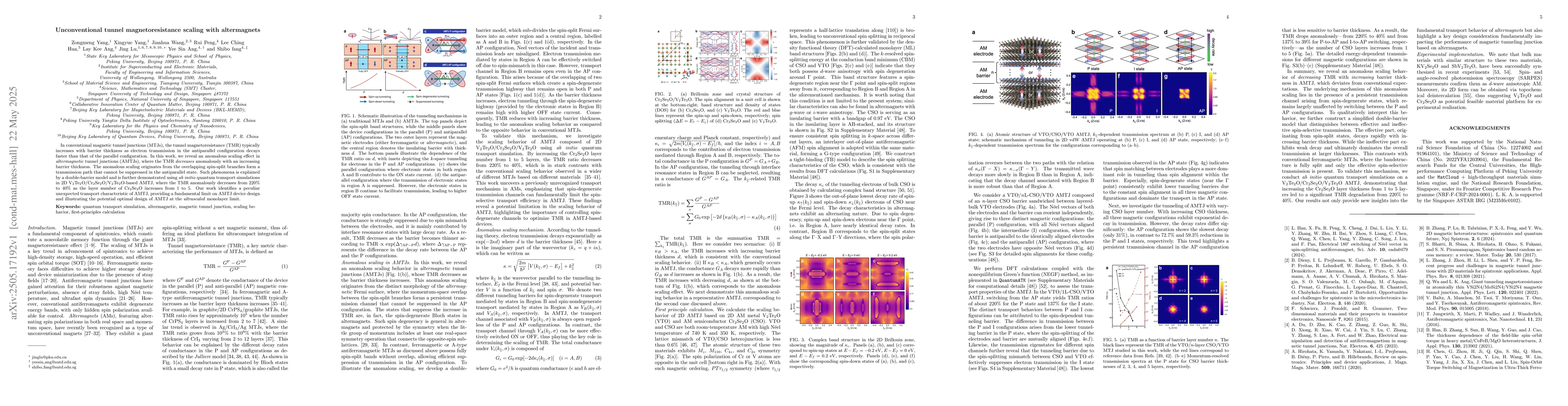
In conventional magnetic tunnel junctions (MTJs), the tunnel magnetoresistance (TMR) typically increases with barrier thickness as electron transmission in the antiparallel configuration decays faster...
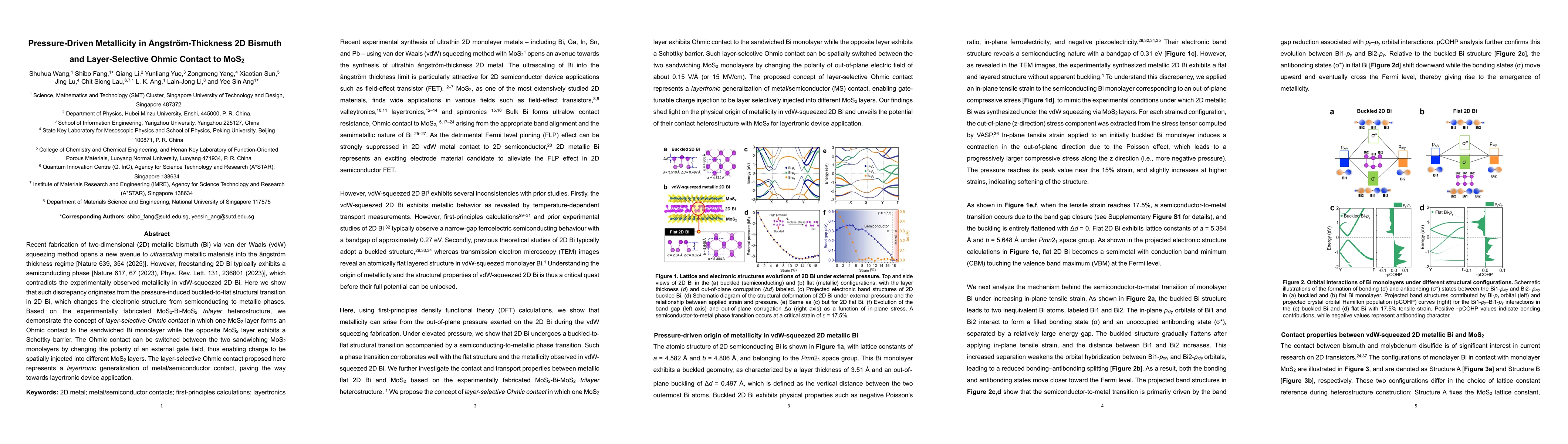
Recent fabrication of two-dimensional (2D) metallic bismuth (Bi) via van der Waals (vdW) squeezing method opens a new avenue to ultrascaling metallic materials into the {\aa}ngstr\"om-thickness regime...
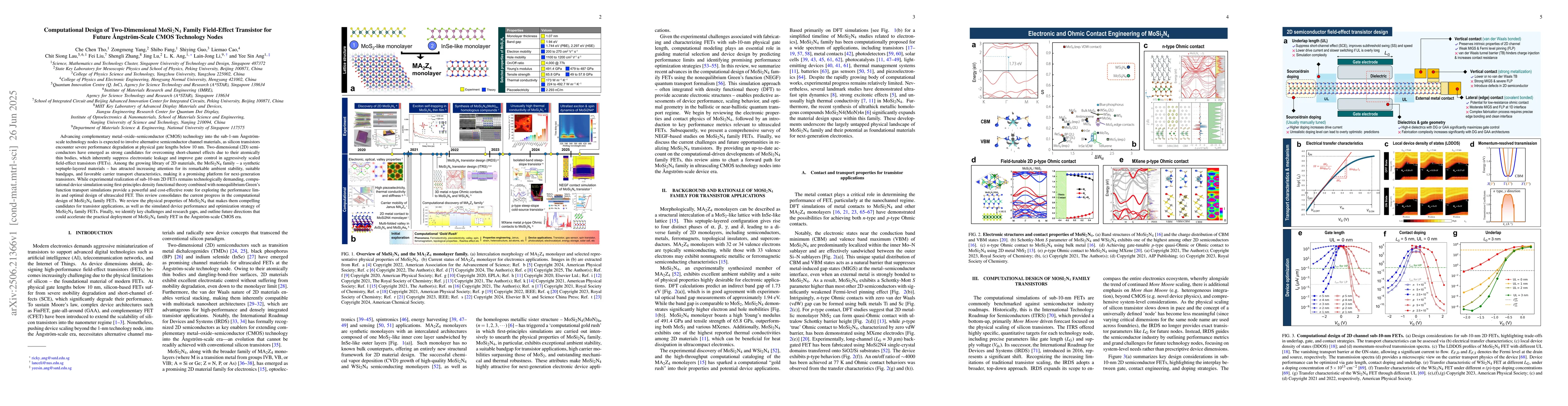
Advancing complementary metal-oxide-semiconductor (CMOS) technology into the sub-1-nm angstr\"om-scale technology nodes is expected to involve alternative semiconductor channel materials, as silicon t...
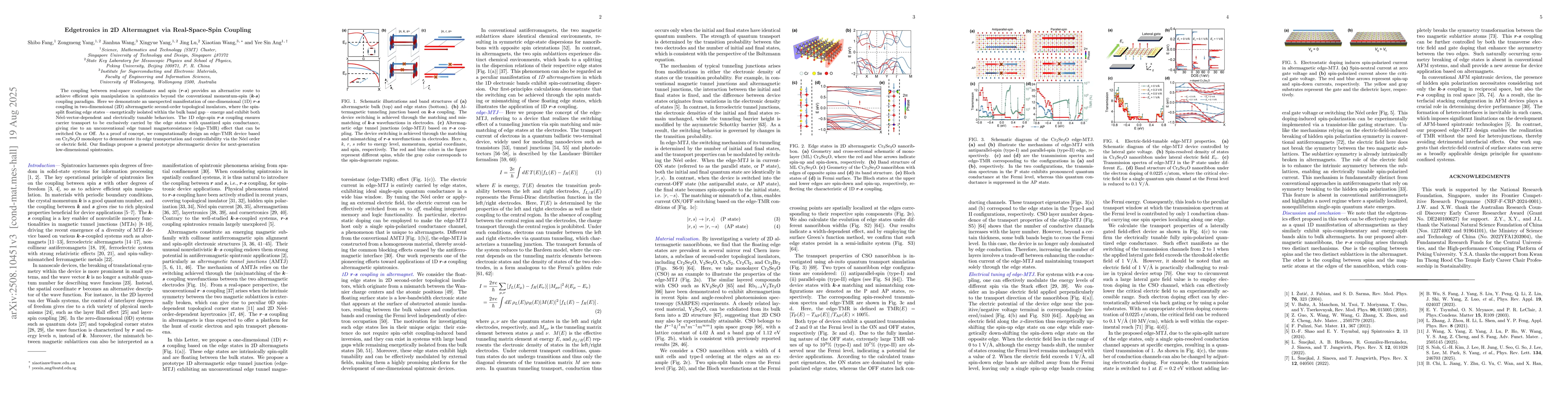
The coupling between real-space coordinates and spin (r-s) provides an alternative route to achieve efficient spin manipulation in spintronics beyond the conventional momentum-spin (k-s) coupling para...
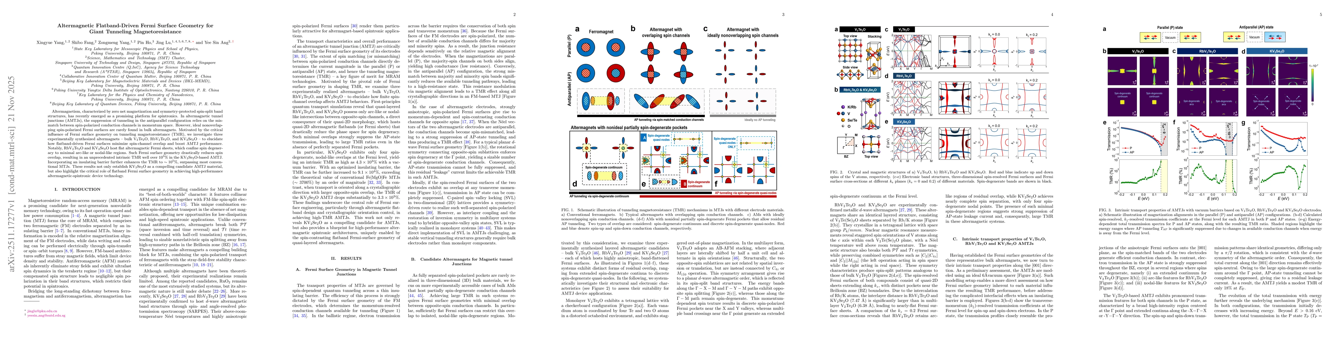
Altermagnetism, characterized by zero net magnetization and symmetry-protected spin-split band structures, has recently emerged as a promising platform for spintronics. In altermagnetic tunnel junctio...
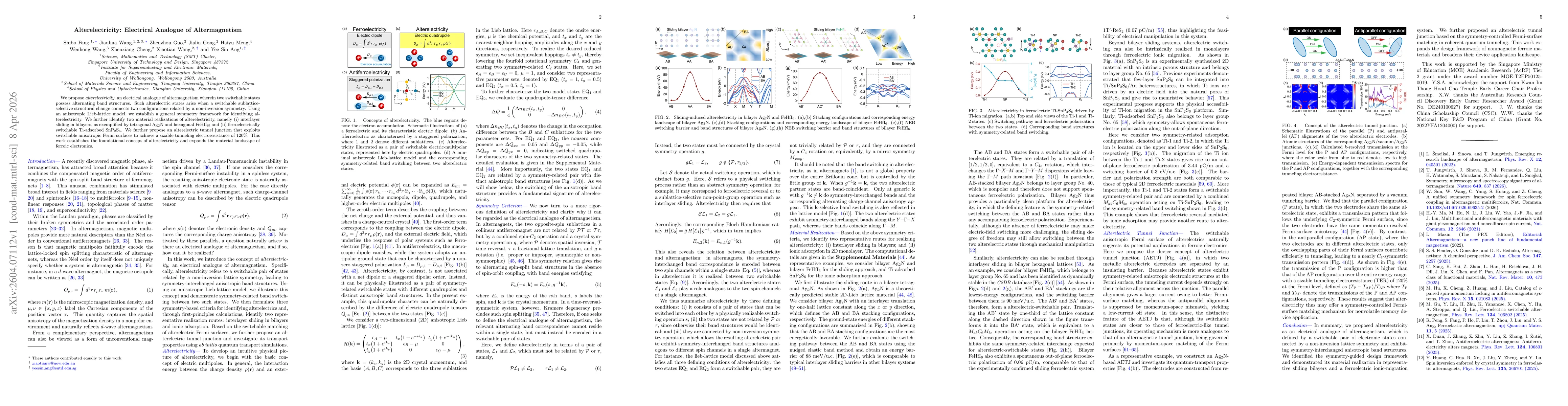
We propose alterelectricity, an electrical analogue of altermagnetism, in which two switchable states possess alternating band structures. Such alterelectric states arise when a switchable sublattice-...
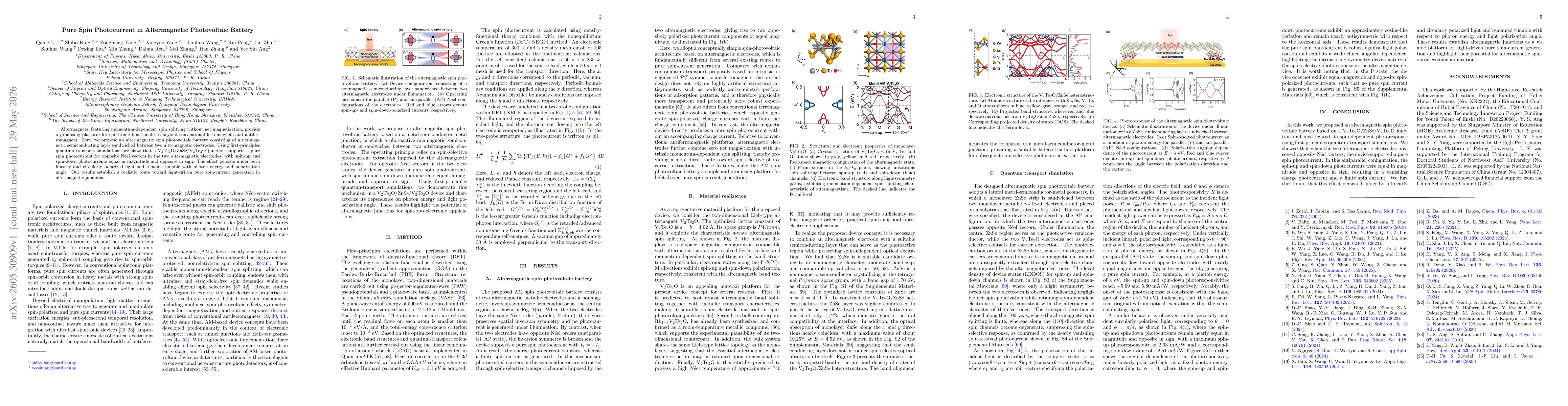
Altermagnets, featuring momentum-dependent spin splitting without net magnetization, provide a promising platform for spintronic functionalities beyond conventional ferromagnets and antiferromagnets. ...