ArxivLens
S
Researcher

Shih-Yuan Wang

10 papers on arXiv

10 arXiv Papers
14 Total Publications
Profile

Academic Profile

Name S. Wang
Total Papers 14
Scholar Profile View on Semantic Scholar
Metrics

Statistics

10 arXiv Papers
14 Total Publications
Publications

Papers on arXiv

Thumbnail for Simulation of Ge on Si Photodiode with photon-trapping micro-nano holes
  with -3dB bandwidth of >60 GHz at NIR wavelength
arXiv
Simulation of Ge on Si Photodiode with photon-trapping micro-nano holes with -3dB bandwidth of >60 GHz at NIR wavelength

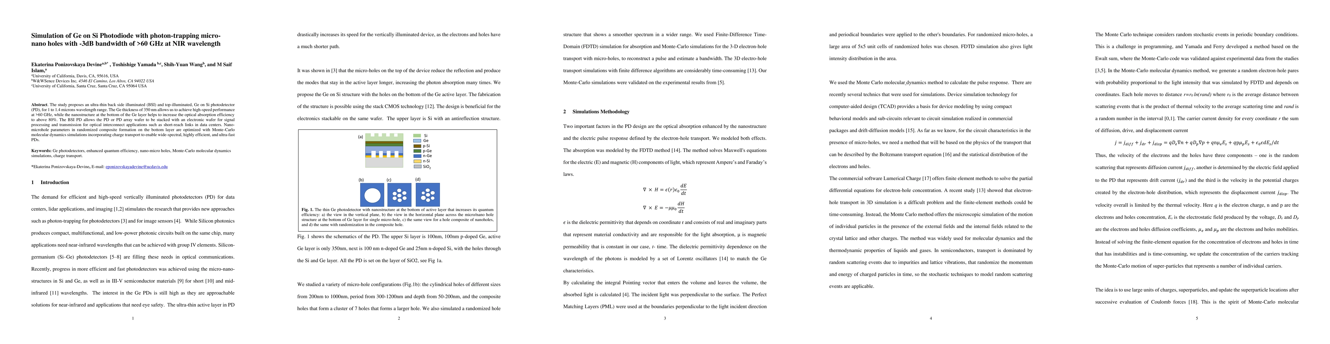
The study proposes an ultra-thin back side illuminated (BSI) and top-illuminated, Ge on Si photodetector (PD), for 1 to 1.4 microns wavelength range. The Ge thickness of 350 nm allows us to achieve ...

Thumbnail for Achieving higher photoabsorption than group III-V semiconductors in
  silicon using photon-trapping surface structures
arXiv
Achieving higher photoabsorption than group III-V semiconductors in silicon using photon-trapping surface structures

The photosensitivity of silicon is inherently very low in the visible electromagnetic spectrum, and it drops rapidly beyond 800 nm in near-infrared wavelengths. Herein, we have experimentally demons...

Thumbnail for CMOS image sensor with micro-nano holes to improve NIR optical
  efficiency: micro-holes on top surface vs on bottom
arXiv
CMOS image sensor with micro-nano holes to improve NIR optical efficiency: micro-holes on top surface vs on bottom

We study the nano- and micro-structures that increase the optical efficiency of the CMOS image pixels in visible and infrared. We consider the difference between the micro-holes at the pixels' botto...

Thumbnail for Single Micro-hole per Pixel for Thin Ge-on-Si Image Sensor with Enhanced
  Sensitivity upto 1700 nm
arXiv
Single Micro-hole per Pixel for Thin Ge-on-Si Image Sensor with Enhanced Sensitivity upto 1700 nm

We present a Ge-on_Si CMOS image sensor with backside illumination for the near-infrared electromagnetic waves, wavelengths range 300-1700nm, detection essential for optical sensor technology. The m...

Thumbnail for Optimizing the light penetration depth in APDs and SPADs for high
  gain-bandwidth and ultra-wide spectral response
arXiv
Optimizing the light penetration depth in APDs and SPADs for high gain-bandwidth and ultra-wide spectral response

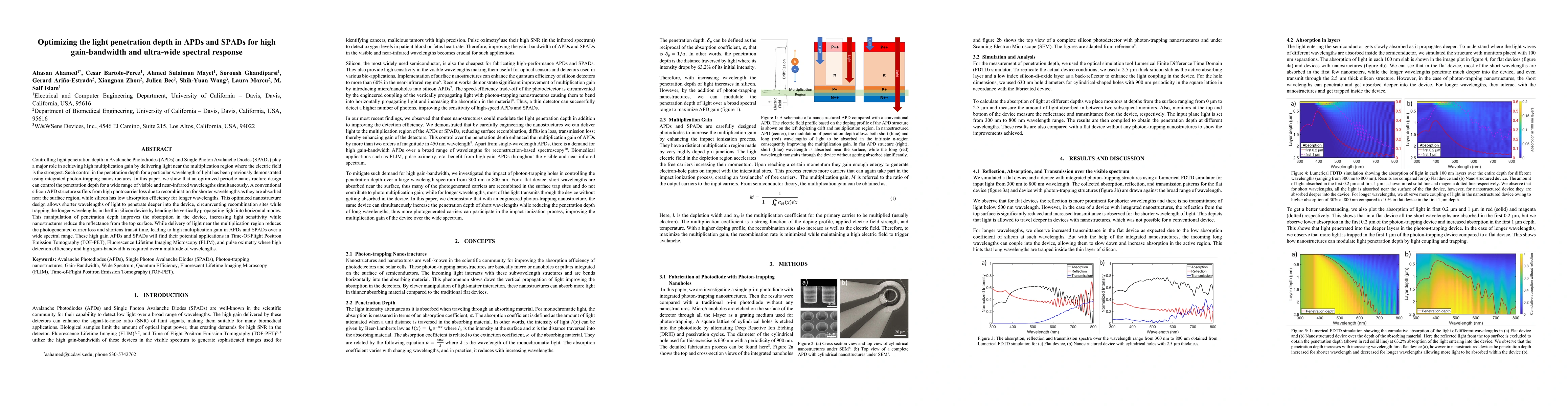
Controlling light penetration depth in Avalanche Photodiodes (APDs) and Single Photon Avalanche Diodes (SPADs) play a major role in achieving high multiplication gain by delivering light near the mu...

Thumbnail for Reconstruction-based spectroscopy using CMOS image sensors with random
  photon-trapping nanostructure per sensor
arXiv
Reconstruction-based spectroscopy using CMOS image sensors with random photon-trapping nanostructure per sensor

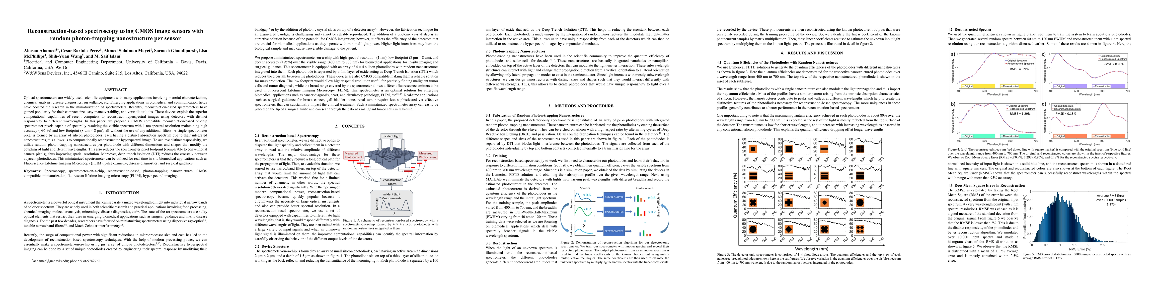
Optical spectrometers are widely used scientific equipment with many applications involving material characterization, chemical analysis, disease diagnostics, surveillance, etc. Emerging application...

Thumbnail for Optimization of CMOS image sensors with single photon-trapping hole per
  pixel for enhanced sensitivity in near-infrared
arXiv
Optimization of CMOS image sensors with single photon-trapping hole per pixel for enhanced sensitivity in near-infrared

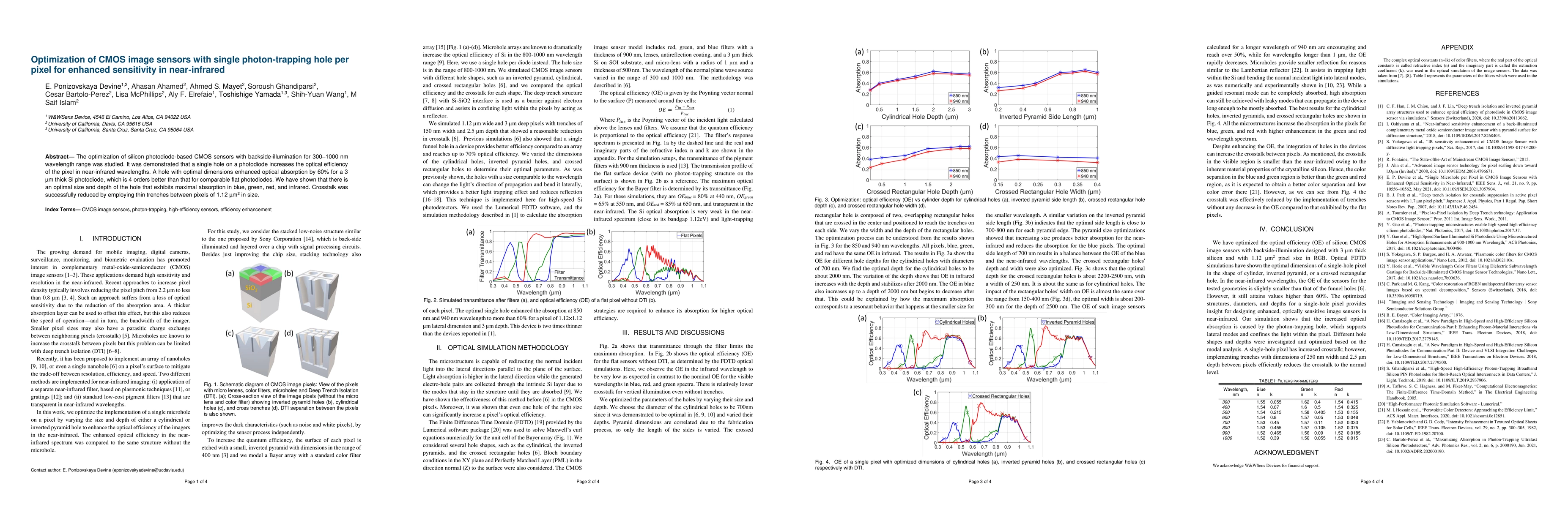
The optimization of silicon photodiode-based CMOS sensors with backside-illumination for 300-1000 nm wavelength range was studied. It was demonstrated that a single hole on a photodiode increases th...

Thumbnail for Avalanche Photodetectors with Photon Trapping Structures for Biomedical
  Imaging Applications
arXiv
Avalanche Photodetectors with Photon Trapping Structures for Biomedical Imaging Applications

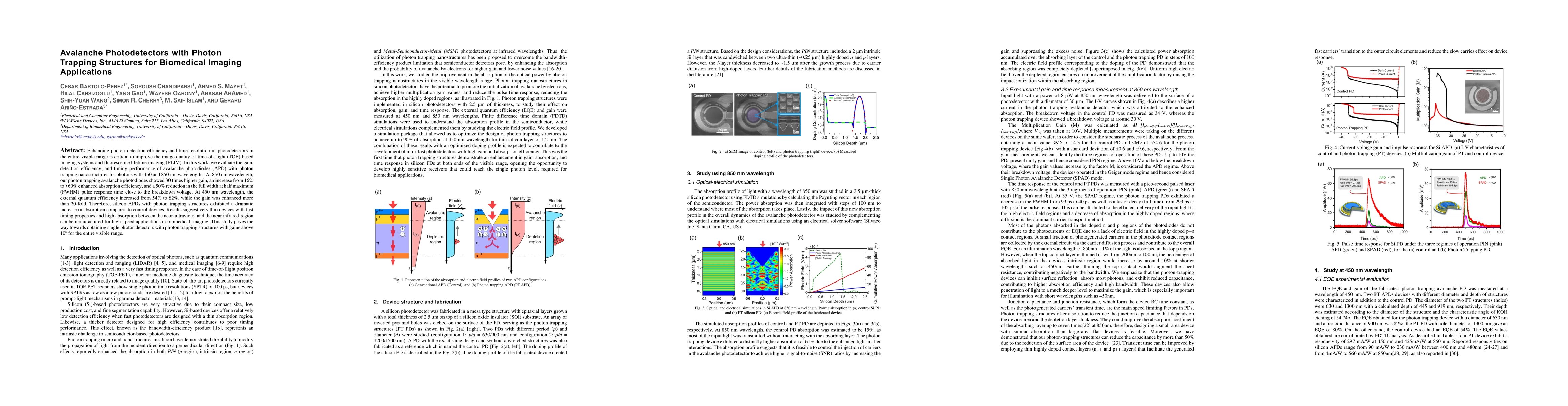
Enhancing photon detection efficiency and time resolution in photodetectors in the entire visible range is critical to improve the image quality of time-of-flight (TOF)-based imaging systems and flu...

Thumbnail for Maximizing absorption in photon trapping ultra-fast silicon
  photodetectors
arXiv
Maximizing absorption in photon trapping ultra-fast silicon photodetectors

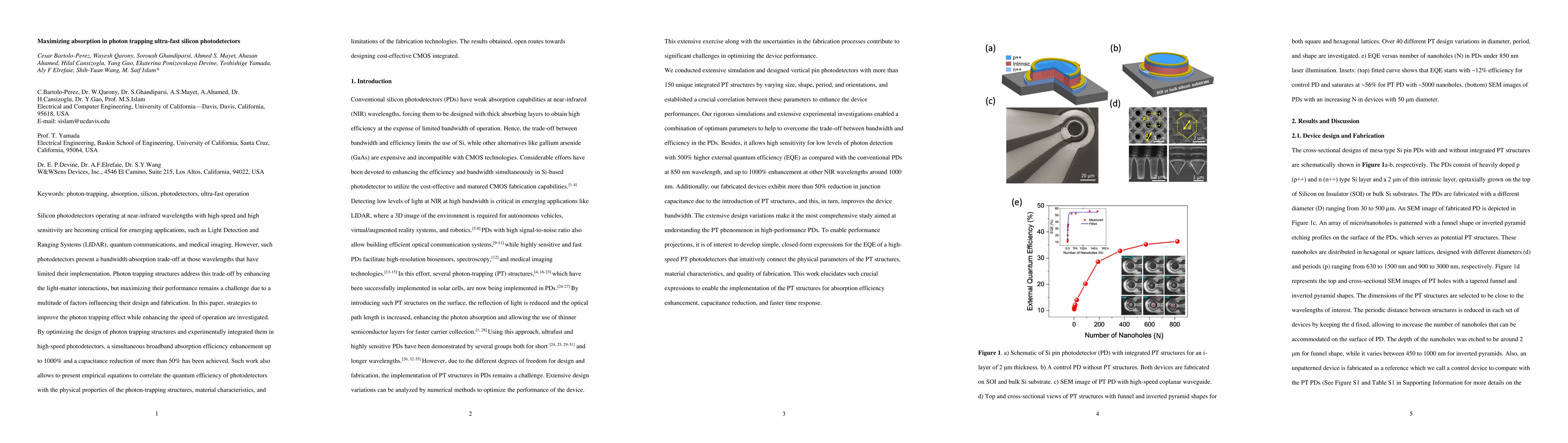
Silicon photodetectors operating at near-infrared wavelengths with high-speed and high sensitivity are becoming critical for emerging applications, such as Light Detection and Ranging Systems (LIDAR...

Thumbnail for Single Microhole per Pixel in CMOS Image Sensor with Enhanced Optical
  Sensitivity in Near-Infrared
arXiv
Single Microhole per Pixel in CMOS Image Sensor with Enhanced Optical Sensitivity in Near-Infrared

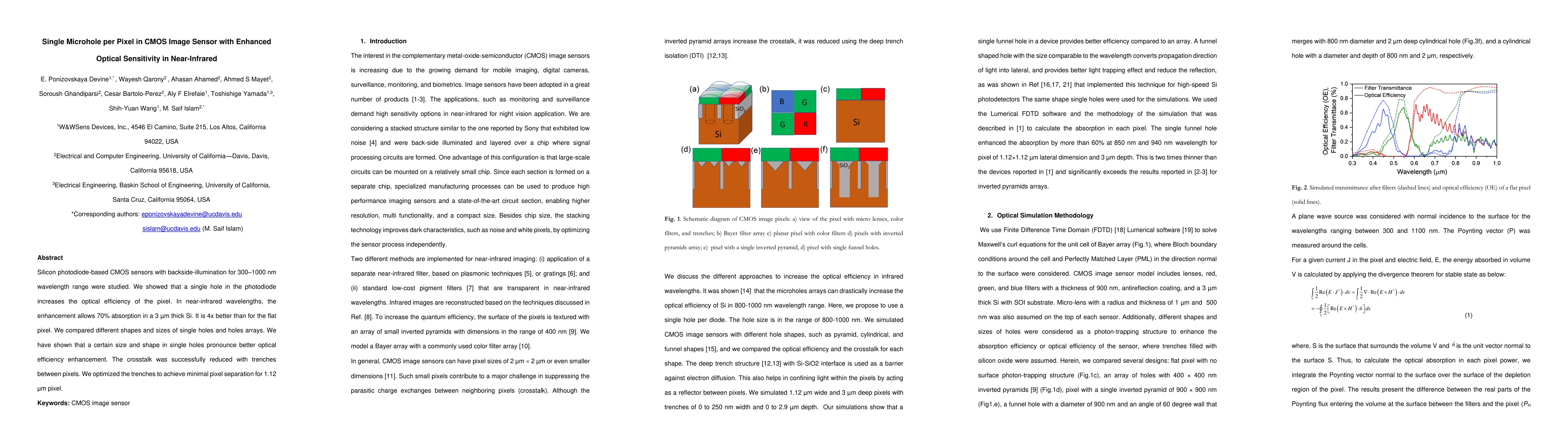
Silicon photodiode based CMOS sensors with backside-illumination for 300 to 1000 nm wavelength range were studied. We showed that a single hole in the photodiode increases the optical efficiency of ...

This website uses cookies to ensure you get the best experience. Learn more