Academic Profile
Statistics
Similar Authors
Papers on arXiv
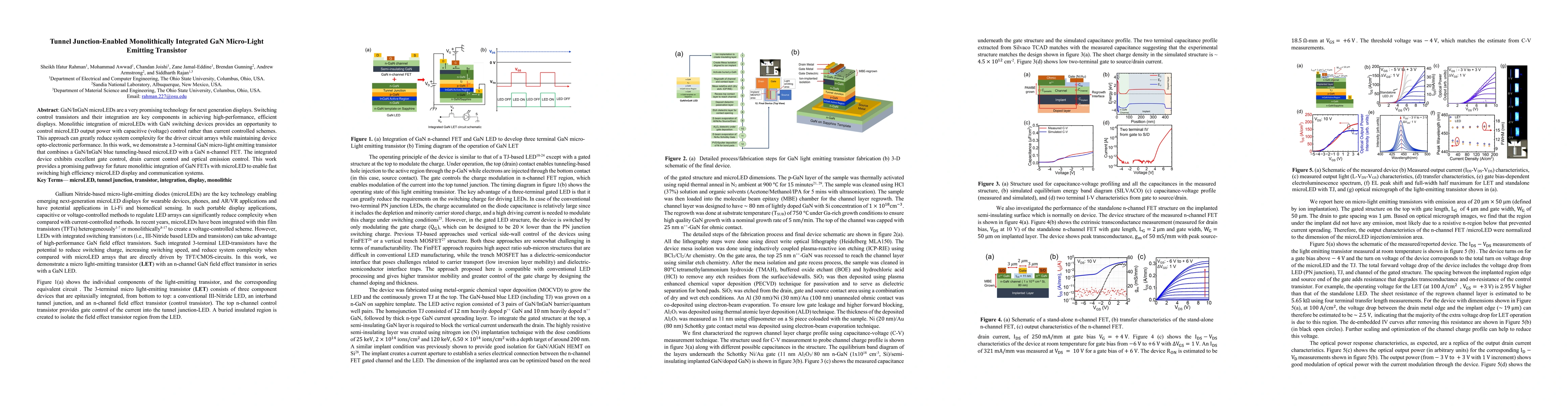
GaN/InGaN microLEDs are a very promising technology for next generation displays. Switching control transistors and their integration are key components in achieving high-performance, efficient disp...
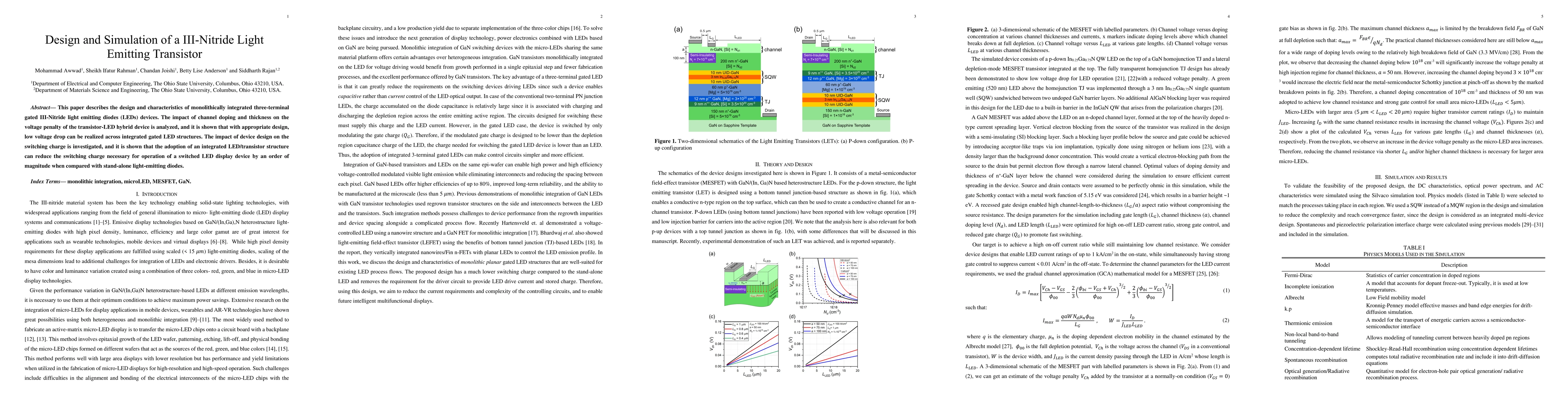
This paper describes the design and characteristics of monolithically integrated three-terminal gated III-Nitride light emitting diodes (LEDs) devices. The impact of channel doping and thickness on ...
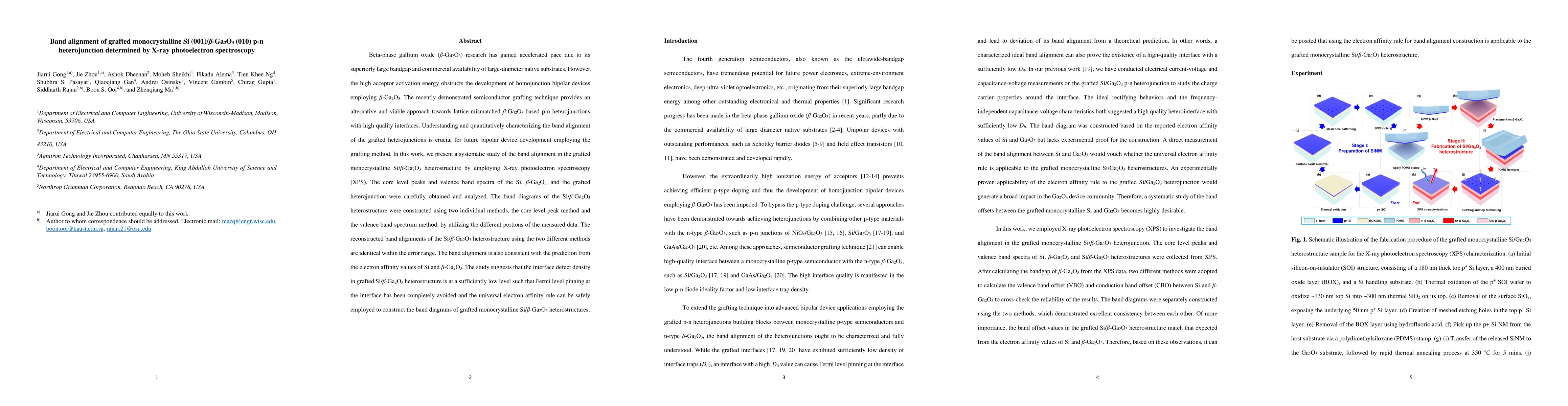
Beta-phase gallium oxide ($\beta$-Ga$_2$O$_3$) research has gained accelerated pace due to its superiorly large bandgap and commercial availability of large-diameter native substrates. However, the ...
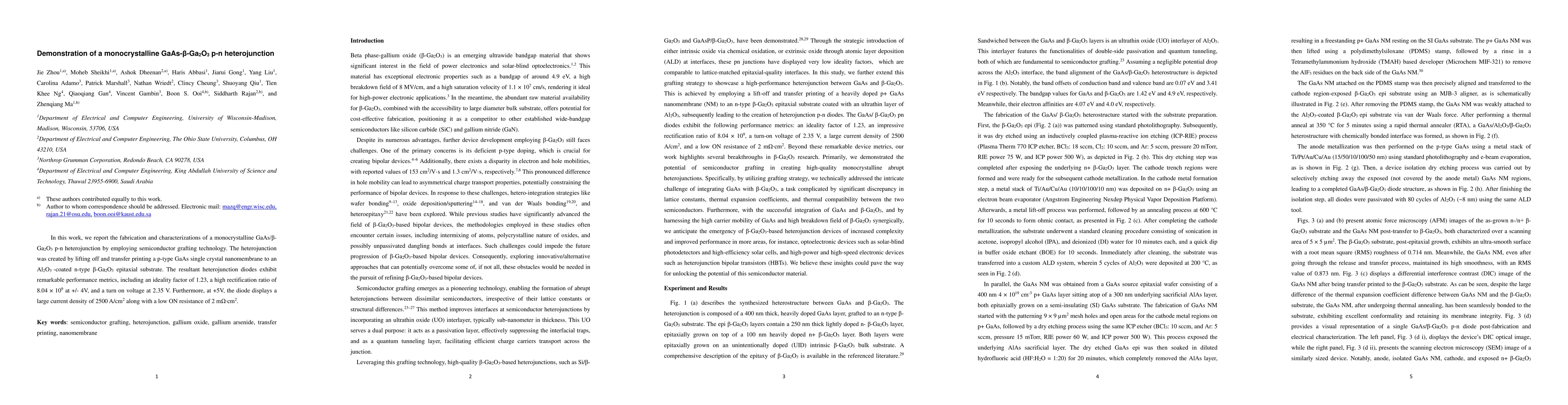
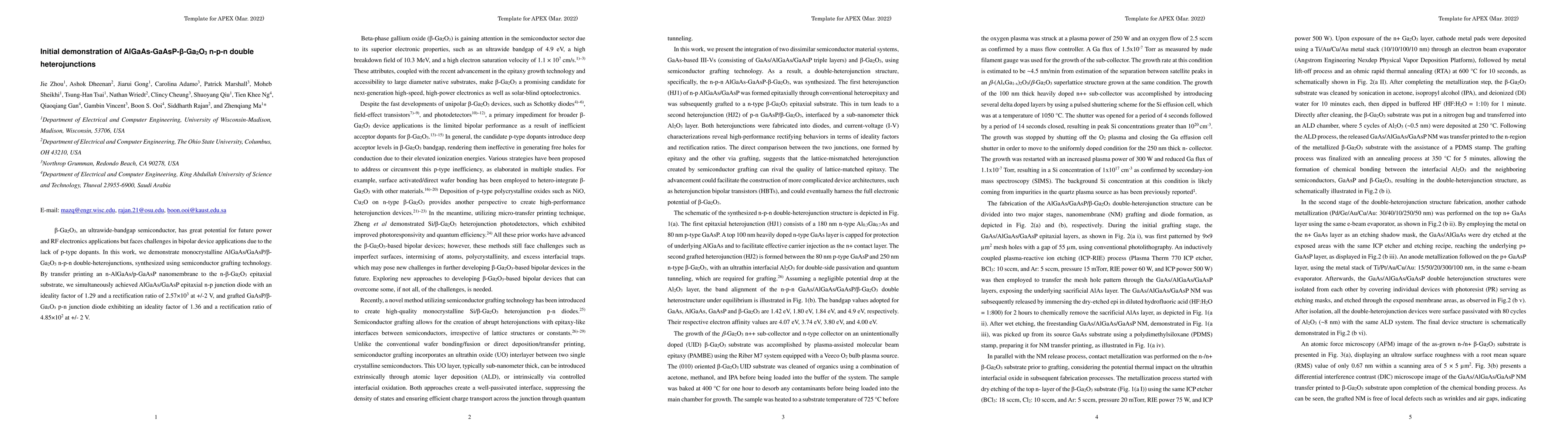
In this work, we report the fabrication and characterizations of a monocrystalline GaAs/$\beta$-Ga$_2$O$_3$ p-n heterojunction by employing semiconductor grafting technology. The heterojunction was ...
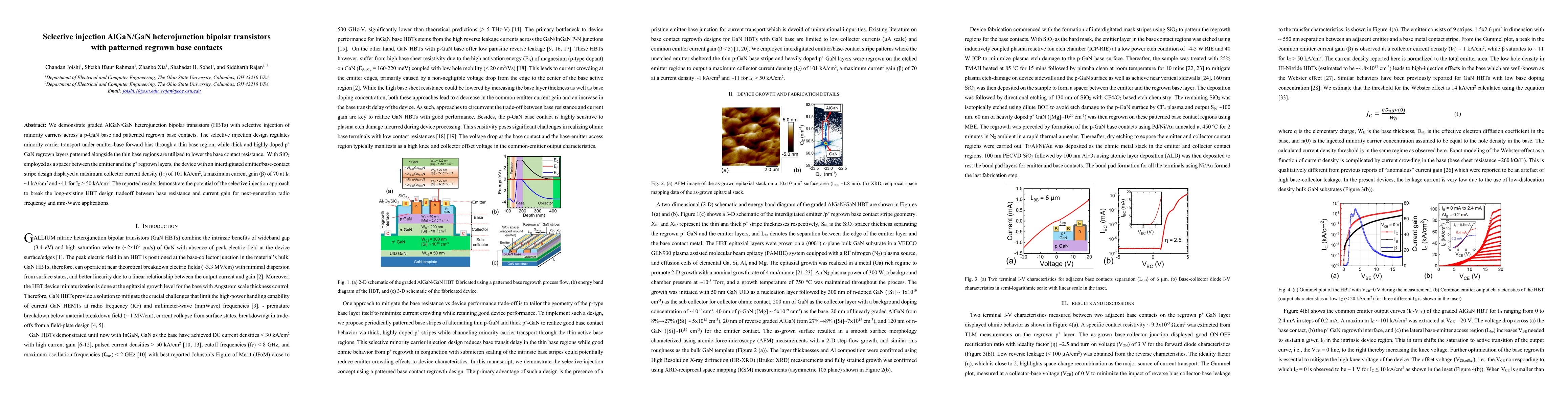
We demonstrate graded AlGaN/GaN heterojunction bipolar transistors (HBTs) with selective injection of minority carriers across a p-GaN base and patterned regrown base contacts. The selective injecti...
Beta phase gallium oxides, an ultrawide-bandgap semiconductor, has great potential for future power and RF electronics applications but faces challenges in bipolar device applications due to the lac...
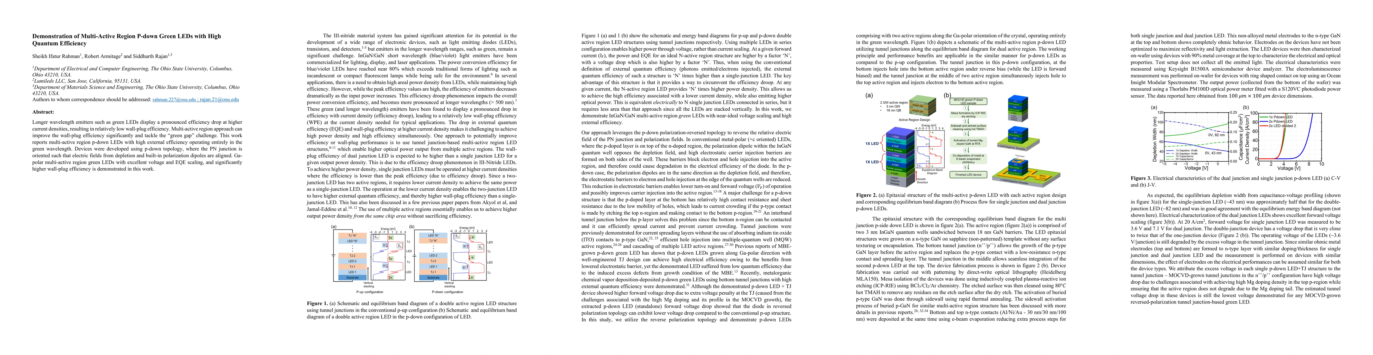
Longer wavelength emitters such as green LEDs display a pronounced efficiency drop at higher current densities, resulting in relatively low wall-plug efficiency. Multi-active region approach can imp...
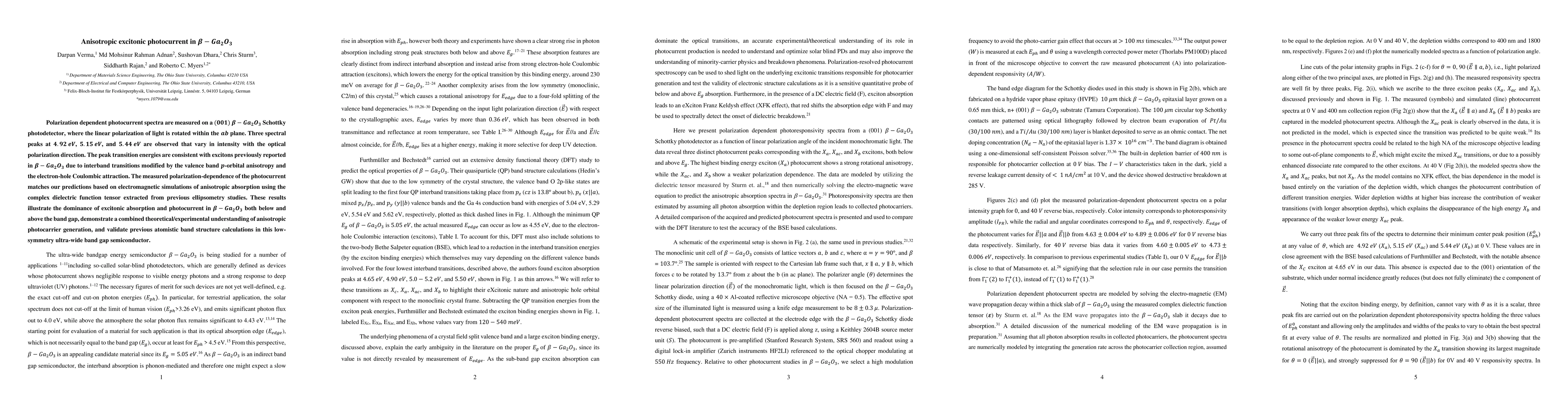
Polarization dependent photocurrent spectra are measured on a (001) $\beta$-Ga$_{2}$O$_{3}$ Schottky photodetector, where the linear polarization of light is rotated within the ab plane. Three spect...
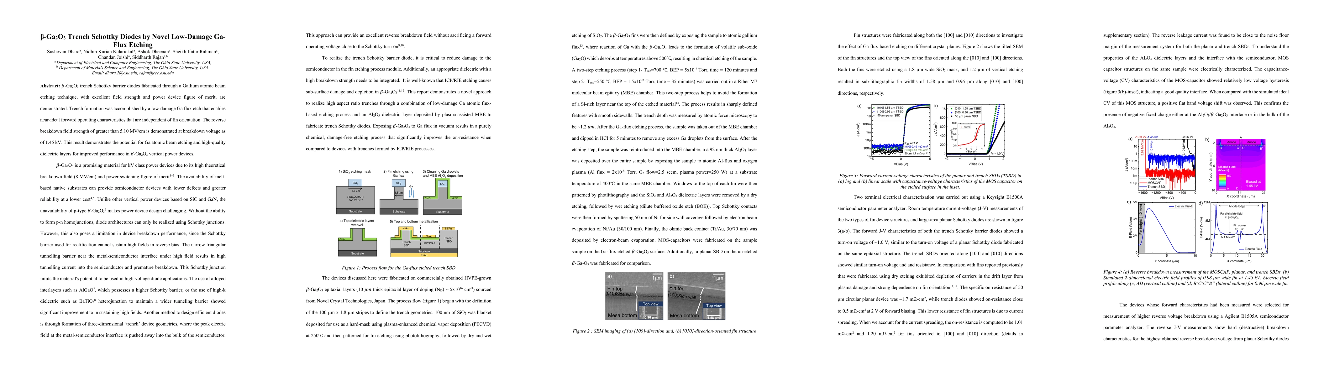
$\beta$-Ga$_2$O$_3$ trench Schottky barrier diodes fabricated through a Gallium atomic beam etching technique, with excellent field strength and power device figure of merit, are demonstrated. Trenc...
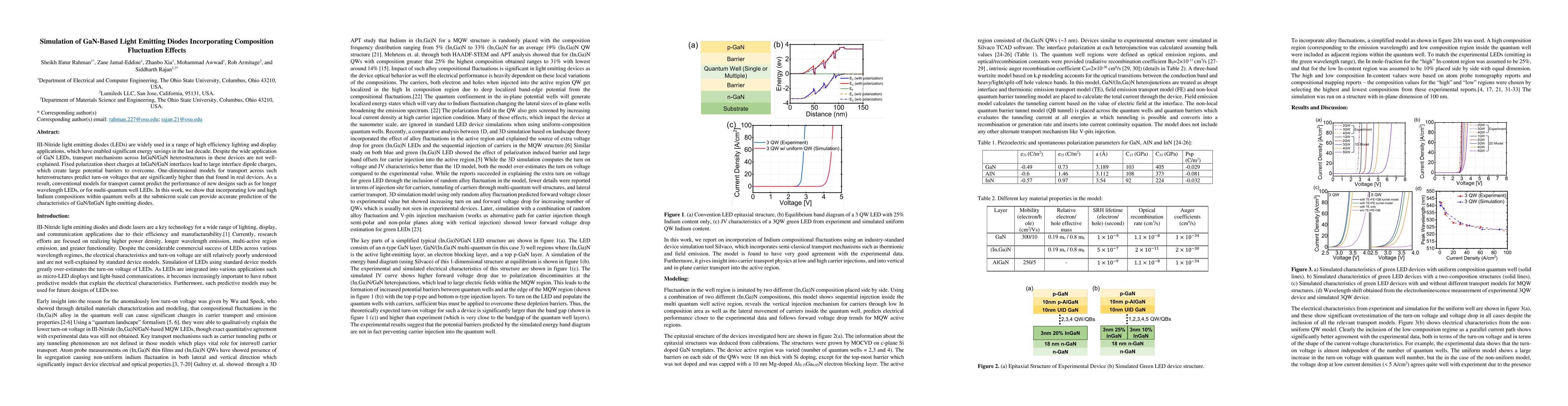
III-Nitride light emitting diodes (LEDs) are widely used in a range of high efficiency lighting and display applications, which have enabled significant energy savings in the last decade. Despite th...
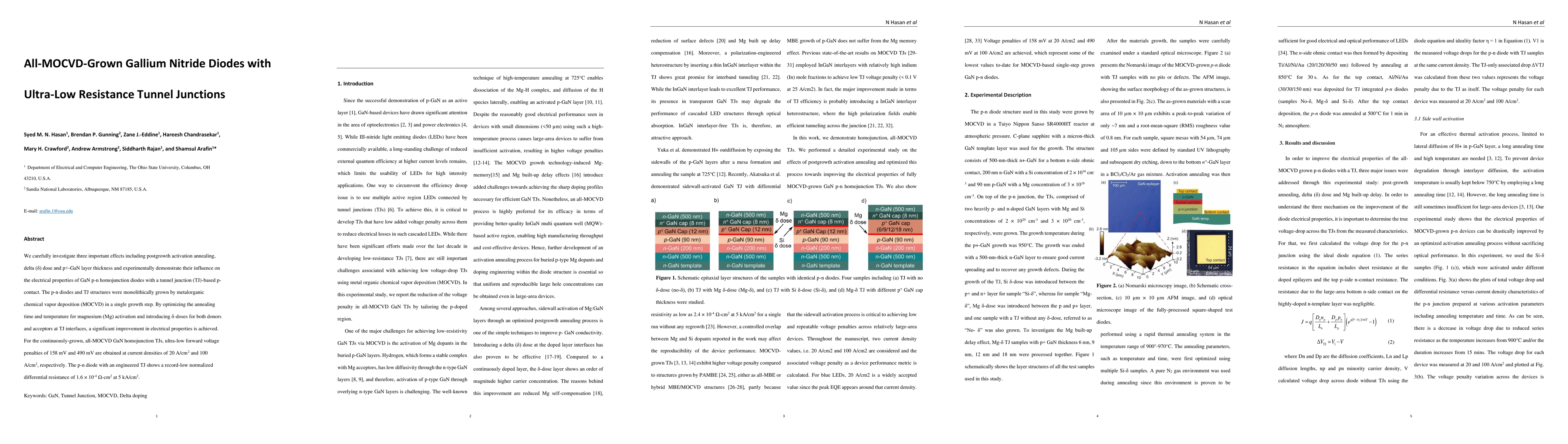
We carefully investigate three important effects including postgrowth activation annealing, delta ({\delta}) dose and p+-GaN layer thickness and experimentally demonstrate their influence on the ele...
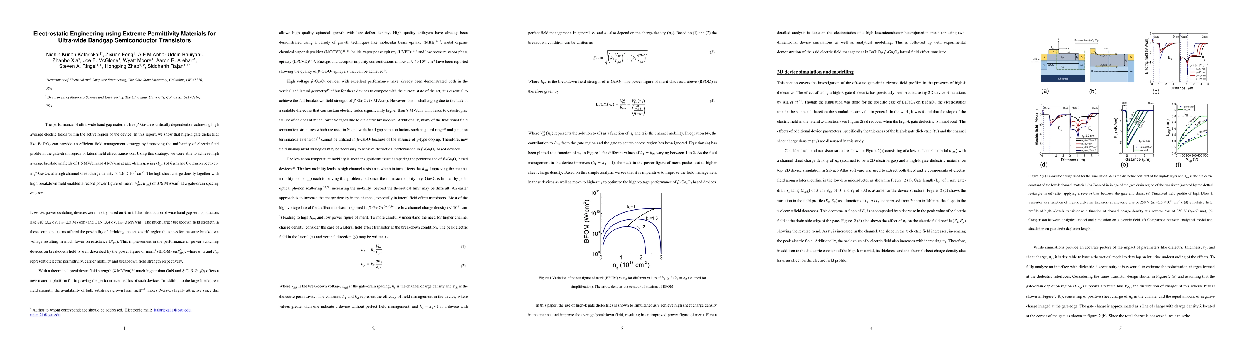
The performance of ultra-wide band gap materials like $\beta$-Ga$_\mathrm{2}$O$_\mathrm{3}$ is critically dependent on achieving high average electric fields within the active region of the device. ...
A new record-high room temperature electron Hall mobility (${\mu}_{RT} = 194\space cm^{2}/V\space s$ at $n\sim 8\times 10^{15}\space cm^{-3}$) for ${\beta}$-Ga2O3 is demonstrated in the unintentiona...
We introduce a deep-recessed gate architecture in $\beta$-Ga$_2$O$_3$ delta-doped field effect transistors for improvement in DC-RF dispersion and breakdown properties. The device design incorporate...
Through magneto-transport measurements and analysis of the observed Shubnikov de Haas oscillations in (010) (AlxGa1-x)2O3/Ga2O3 heterostructures, spin-splitting of the Landau levels in the (010) Ga2...
Wide and ultra-wide band gap semiconductors can provide excellent performance due to their high energy band gap, which leads to breakdown electric fields that are more than an order of magnitude hig...
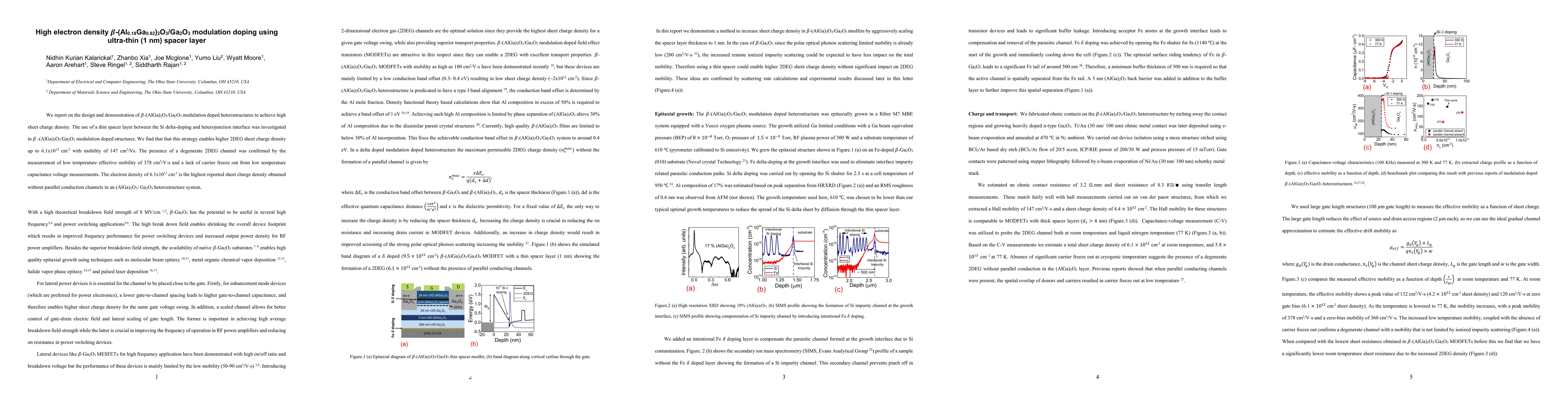
We report on the design and demonstration of ${\beta}-(Al_{0.18}Ga_{0.82})_2O_3/Ga_2O_3$ modulation doped heterostructures to achieve high sheet charge density. The use of a thin spacer layer betwee...
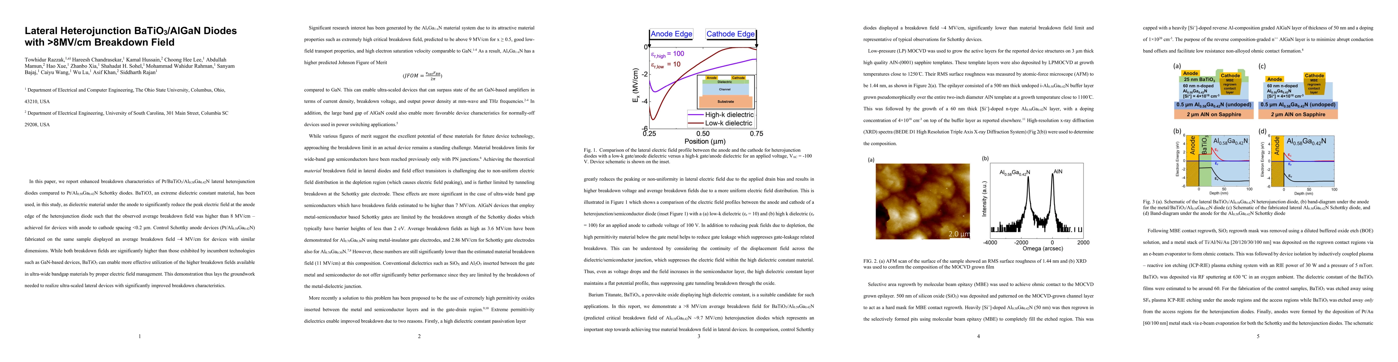
In this paper, we report enhanced breakdown characteristics of Pt/BaTiO3/Al0.58Ga0.42N lateral heterojunction diodes compared to Pt/Al0.58Ga0.42N Schottky diodes. BaTiO3, an extreme dielectric const...
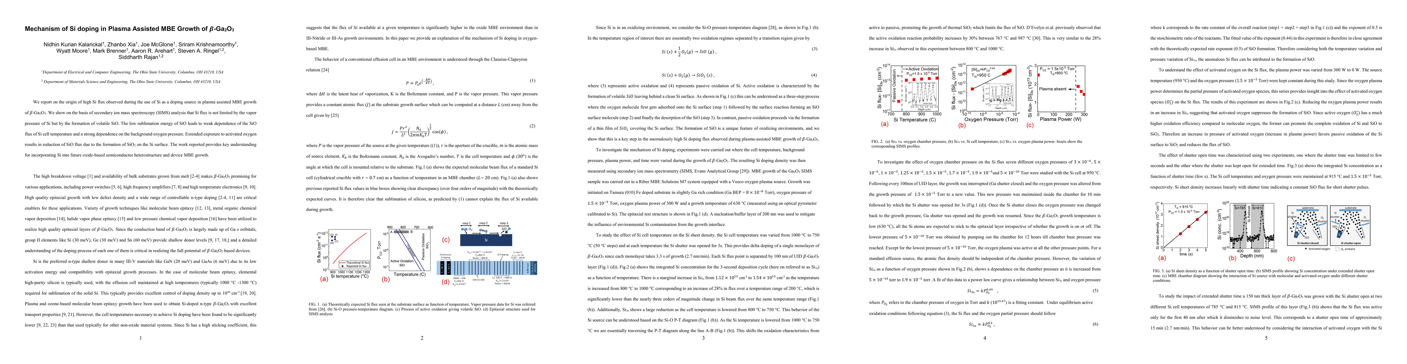
We report on the origin of high Si flux observed during the use of Si as a doping source in plasma assisted MBE growth of \b{eta}-Ga2O3. We show on the basis of secondary ion mass spectroscopy (SIMS...
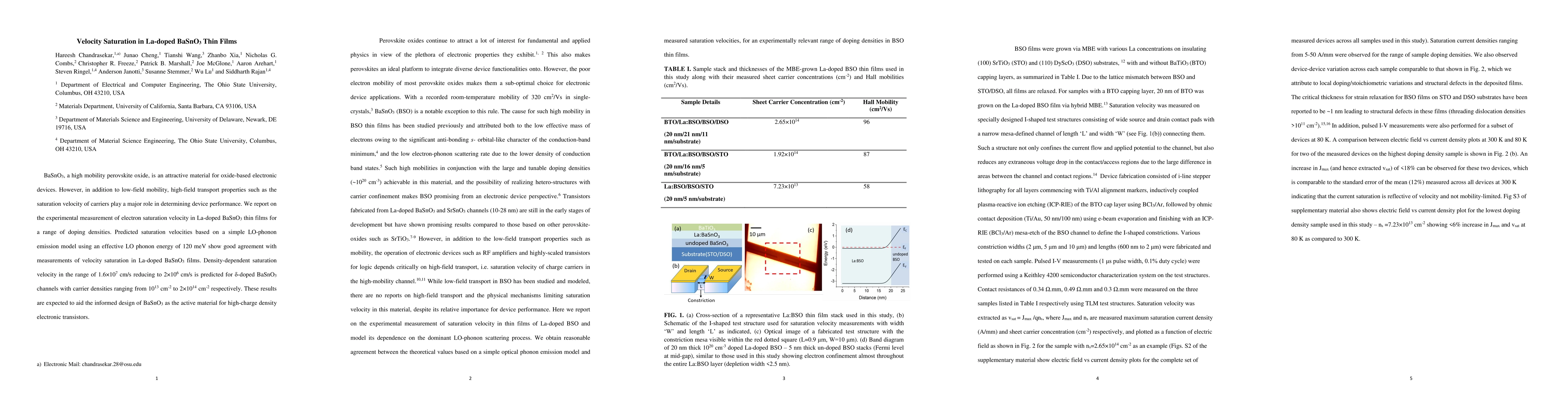
BaSnO_{3}, a high mobility perovskite oxide, is an attractive material for oxide-based electronic devices. However, in addition to low-field mobility, high-field transport properties such as the sat...
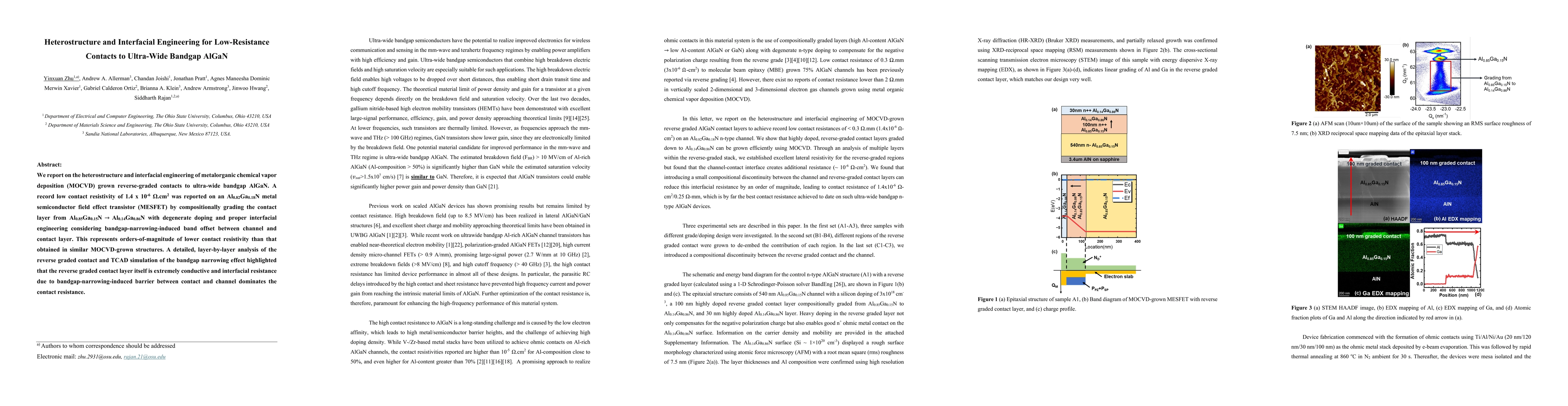
We report on the heterostructure and interfacial engineering of metalorganic chemical vapor deposition (MOCVD) grown reverse-graded contacts to ultra-wide bandgap AlGaN. A record low contact resistivi...
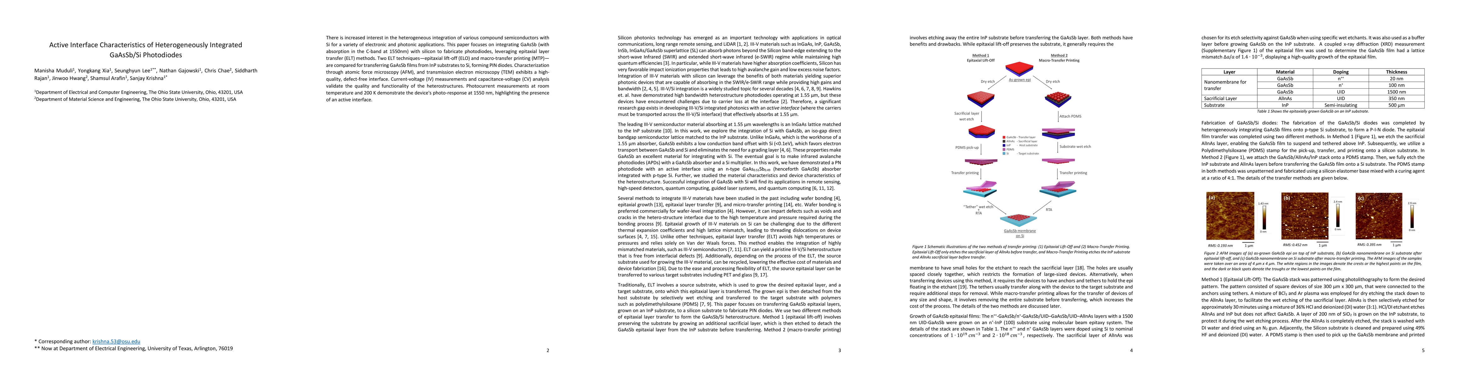
There is increased interest in the heterogeneous integration of various compound semiconductors with Si for a variety of electronic and photonic applications. This paper focuses on integrating GaAsSb ...
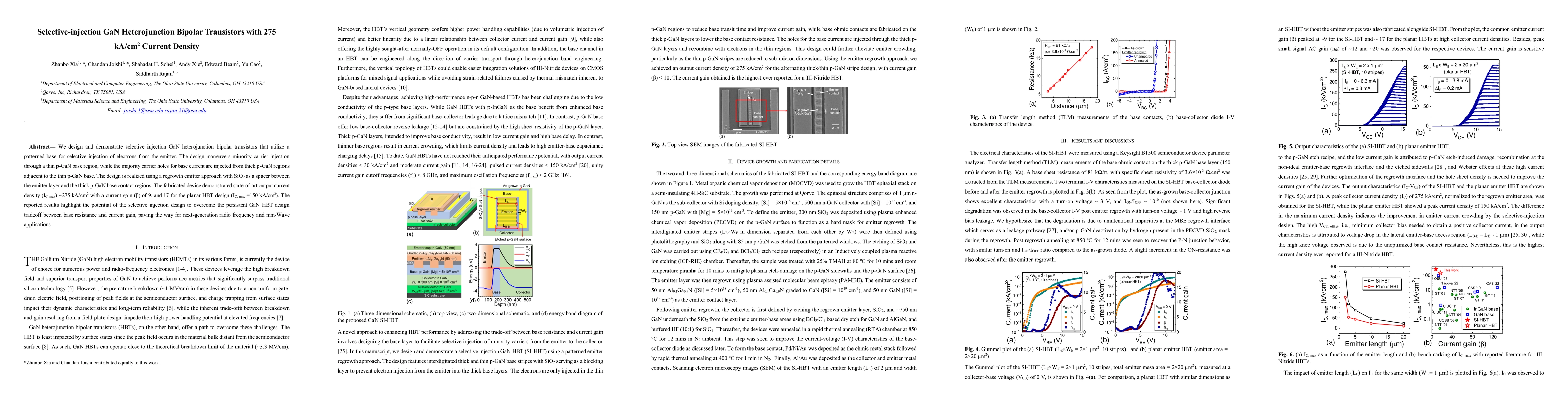
We design and demonstrate selective injection GaN heterojunction bipolar transistors that utilize a patterned base for selective injection of electrons from the emitter. The design maneuvers minority ...
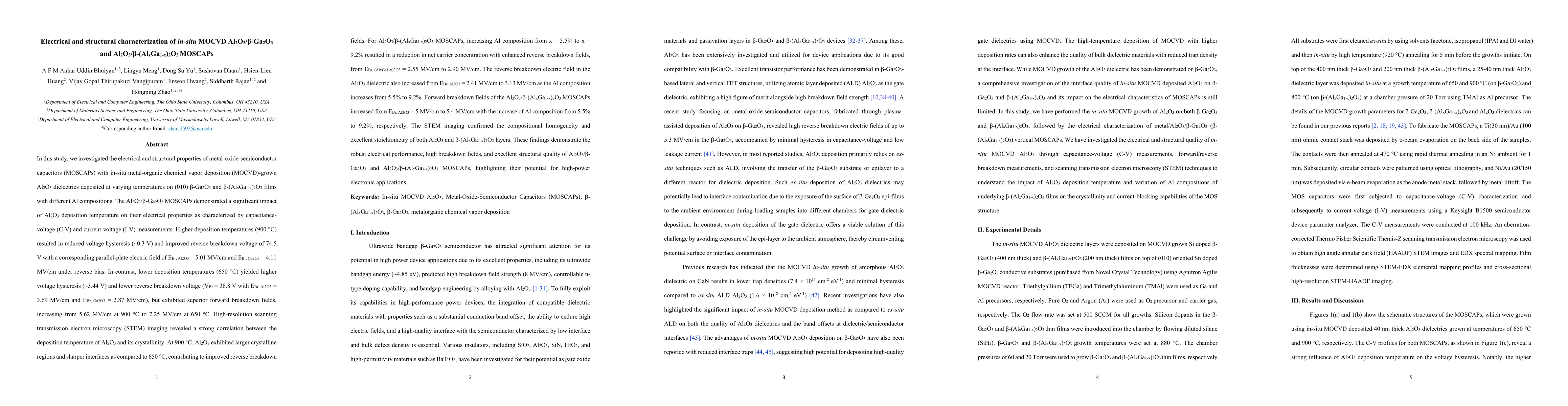
This study investigates the electrical and structural properties of MOSCAPs with in-situ MOCVD-grown Al$_2$O$_3$ dielectrics on (010) $\beta$-Ga$_2$O$_3$ and $\beta$-(Al$_x$Ga$_{1-x}$)$_2$O$_3$ films....
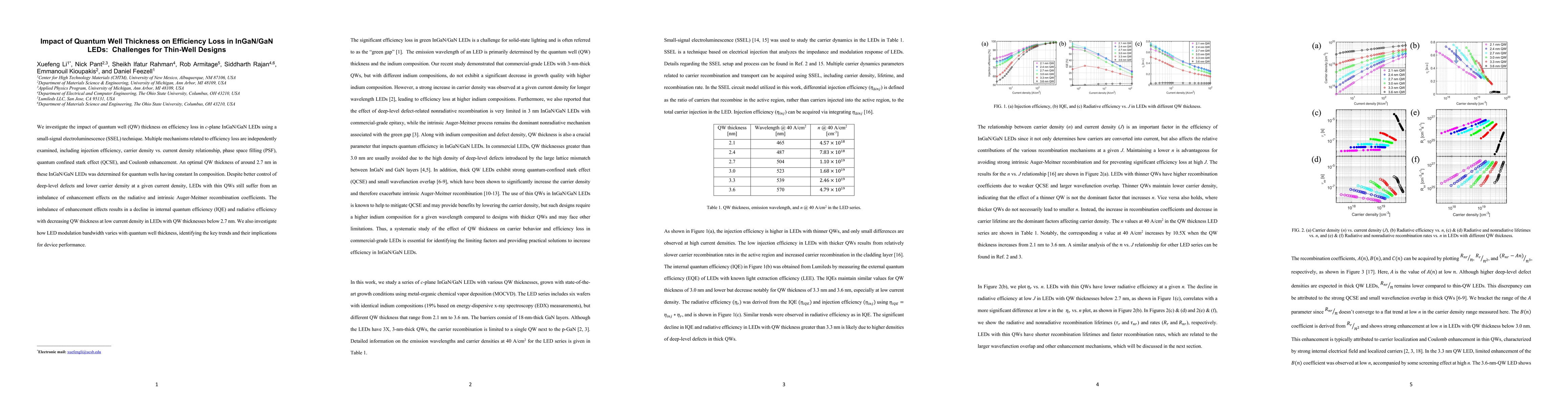
We investigate the impact of quantum well (QW) thickness on efficiency loss in c-plane InGaN/GaN LEDs using a small-signal electroluminescence (SSEL) technique. Multiple mechanisms related to efficien...
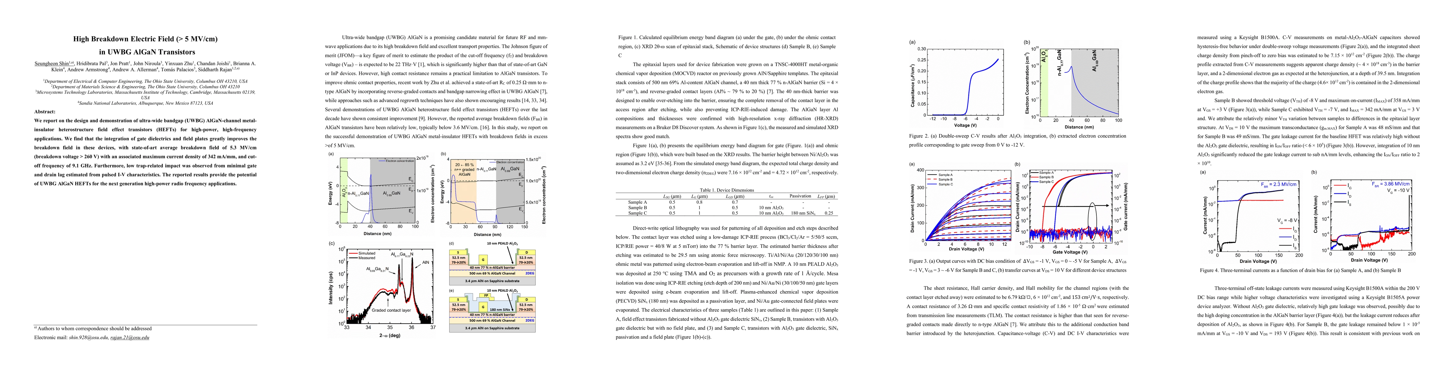
We report on the design and demonstration of ultra-wide bandgap (UWBG) AlGaN-channel metal-insulator heterostructure field effect transistors (HEFTs) for high-power, high-frequency applications. We fi...
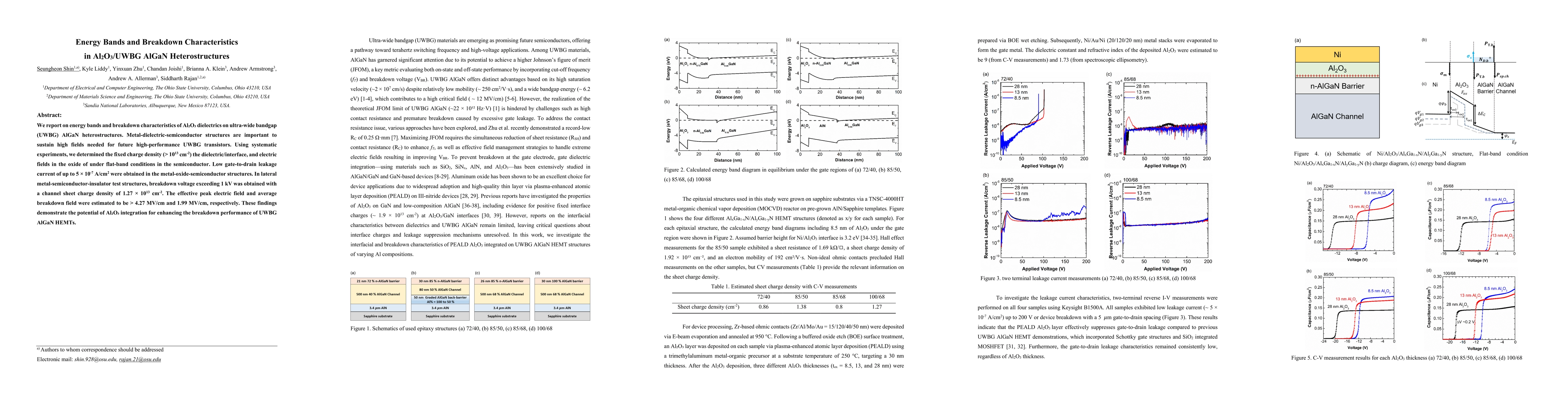
We report on energy bands and breakdown characteristics of Al2O3 dielectrics on ultra-wide bandgap (UWBG) AlGaN heterostructures. Metal-dielectric-semiconductor structures are important to sustain hig...
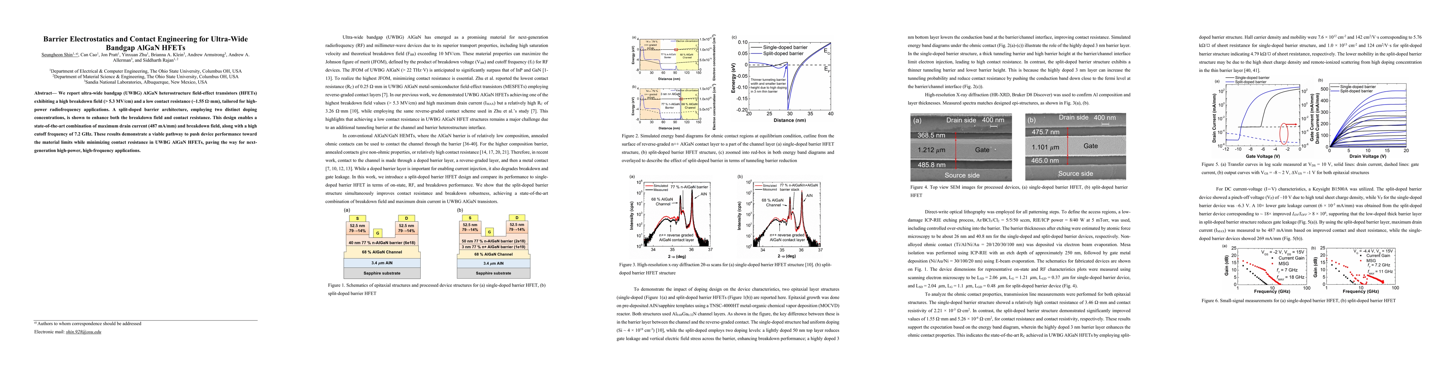
We report ultra-wide bandgap (UWBG) AlGaN heterostructure field-effect transistors (HFETs) exhibiting a high breakdown field (> 5.3 MV/cm) and a low contact resistance (~1.55 {\Omega}mm), tailored for...
To investigate the scope of ferroelectric behavior in La-substituted BiFeO3 films, LaxBi1-xFeO3 epitaxial films were synthesized using off-axis co-sputtering on SrTiO3(001) and DyScO3(110) substrates ...
We report on the design and demonstration of ultra-wide bandgap AlGaN polarization-graded field effect transistors with ultra-thin channels to enable excellent current density and high-frequency perfo...
We report the design and demonstration of ultra-wide-bandgap (UWBG) AlGaN polarization-graded field-effect transistors (PolFETs) that achieve a current-gain cutoff frequency above 85 GHz and a current...
Next-generation high-power radio-frequency (RF) devices increasingly demand transistors that operate efficiently with high gain at high frequencies. High-aluminum-content ultra-wide-bandgap (UWBG) AlG...
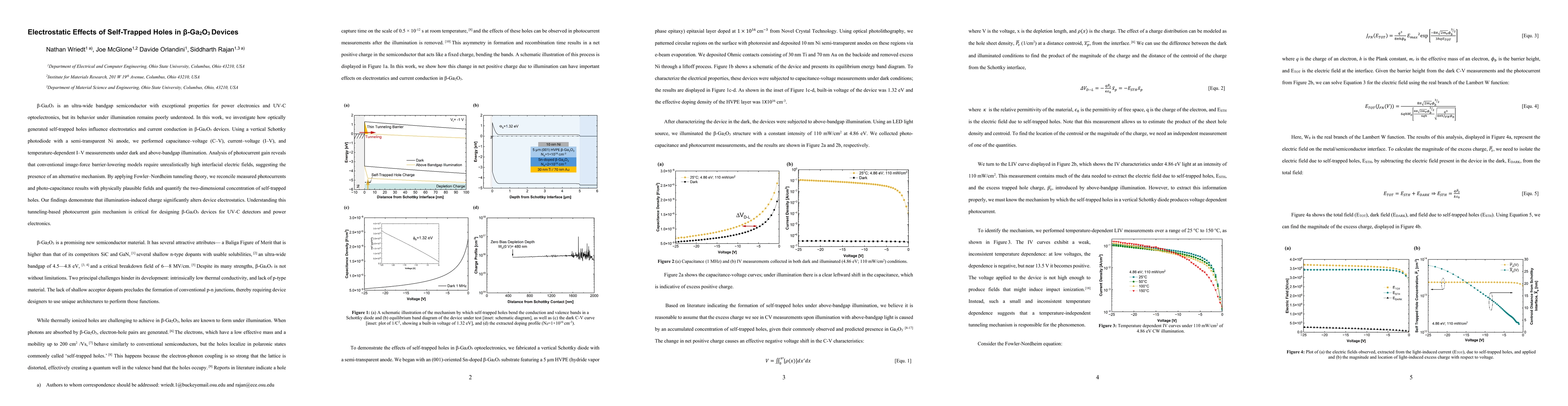
Gallium oxide is an ultra-wide bandgap semiconductor with exceptional properties for power electronics and UV-C optoelectronics, but its behavior under illumination remains poorly understood. In this ...
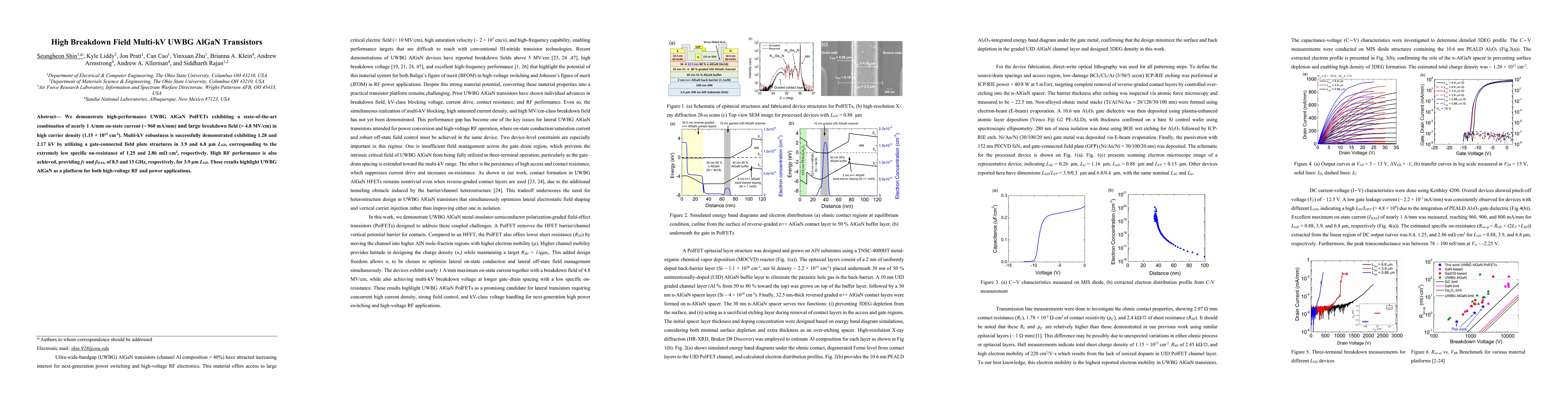
We demonstrate high-performance UWBG AlGaN PolFETs exhibiting a state-of-the-art combination of nearly 1 A/mm on-state current (~ 960 mA/mm) and large breakdown field (> 4.8 MV/cm) in high carrier den...
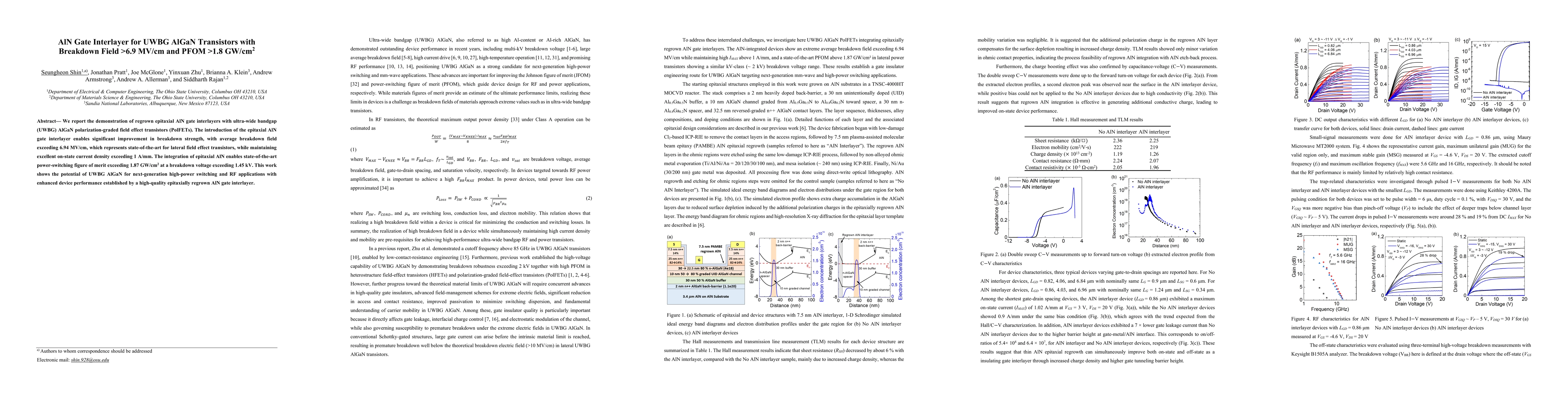
We report the demonstration of regrown epitaxial AlN gate interlayers with ultra-wide bandgap (UWBG) AlGaN polarization-graded field effect transistors (PolFETs). The introduction of the epitaxial AlN...