Academic Profile
Statistics
Similar Authors
Papers on arXiv
Doped semiconductors are a central and crucial component of all integrated circuits. By using a combination of white light and a focused laser beam, and exploiting hBN defect states, heterostructure...
Emerging low-dimensional nanomaterials have been studied for decades in device applications as field-effect transistors (FETs). However, properly reporting and comparing device performance has been ...
The emergence of interference is observed in the resistance of a graphene annulus pn junction device as a result of applying two separate gate voltages. The observed resistance patterns are carefull...
We demonstrate a high capacity IF-over-fiber mobile fronthaul solution for multi-user massive MIMO 5G RAN. Using this scheme, a record aggregated radio bandwidth of 25.6 GHz was transmitted on a sin...
The quantum Hall (QH) effect, a topologically non-trivial quantum phase, expanded and brought into focus the concept of topological order in physics. The topologically protected quantum Hall edge st...
We show that simple, commercially sourced n-channel silicon field-effect transistors (nFETs) operating under closed loop control exhibit an ~3-fold improvement in pH readout resolution to (7.2+/-0.3...
We have demonstrated atomically thin, quantum capacitance-limited, field-effect transistors (FETs) that enable the detection of pH changes with ~75-fold higher sensitivity (4.4 V/pH) over the Nernst...
Advancements in fabrication methods have shaped new computing device technologies. Among these methods, depositing electrical contacts to the channel material is fundamental to device characterization...
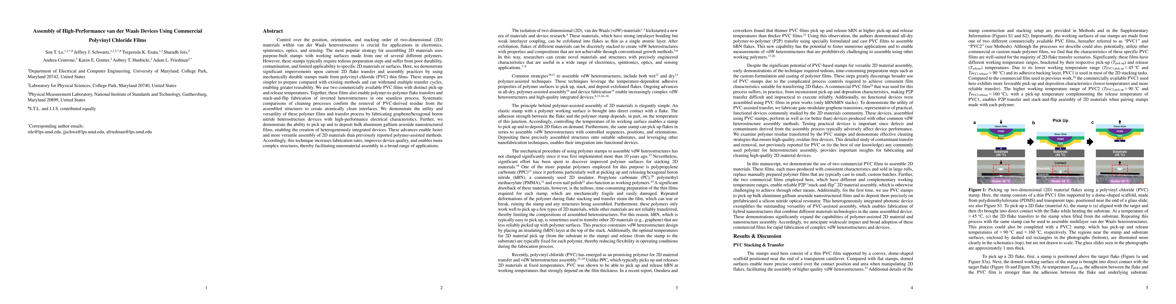
Control over the position, orientation, and stacking order of two-dimensional (2D) materials within van der Waals heterostructures is crucial for applications in electronics, spintronics, optics, and ...
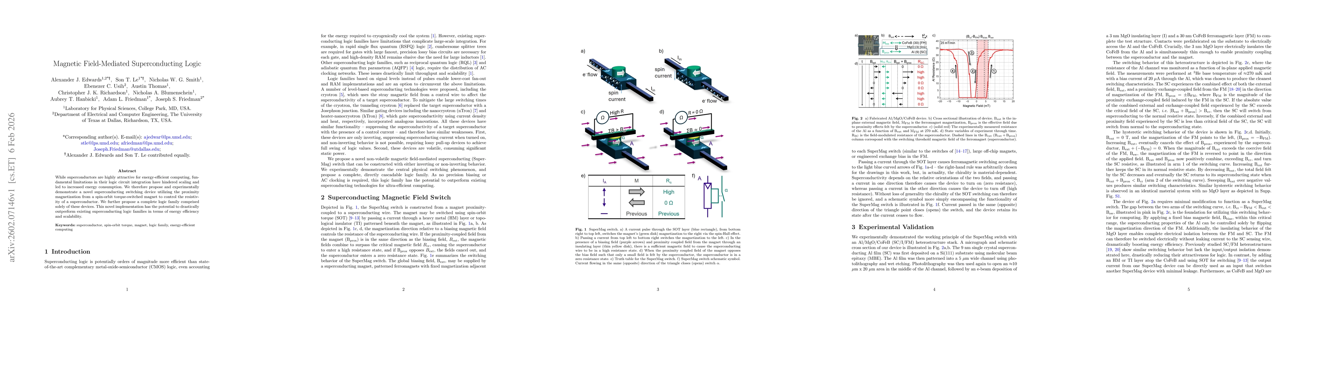
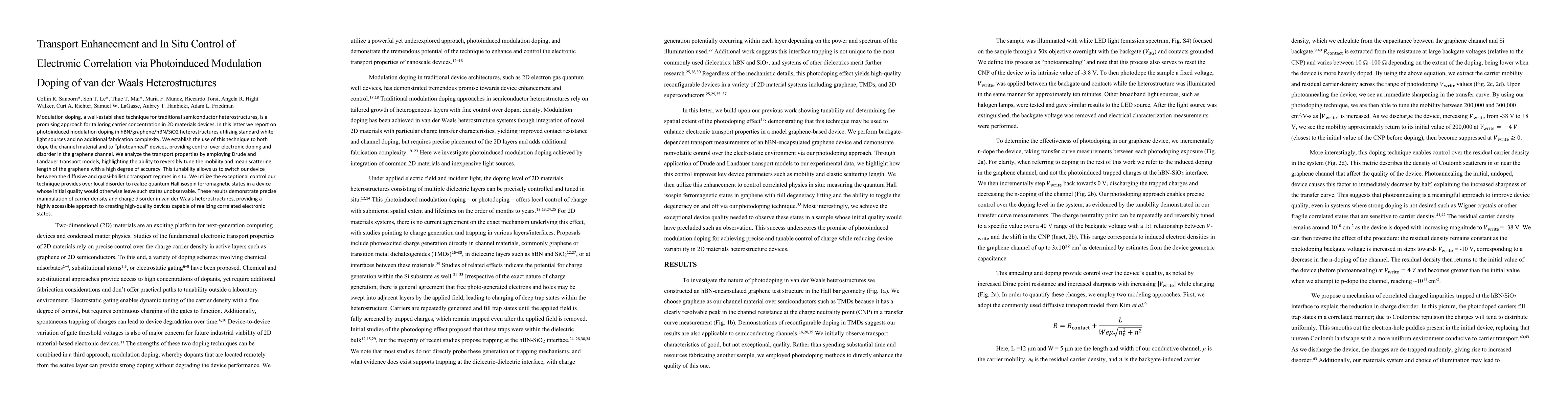
While superconductors are highly attractive for energy-efficient computing, fundamental limitations in their logic circuit integration have hindered scaling and led to increased energy consumption. We...
Modulation doping, a well-established technique for traditional semiconductor heterostructures, is a promising approach for tailoring carrier concentration in 2D materials devices. In this letter we r...