Academic Profile
Statistics
Similar Authors
Papers on arXiv
Femtosecond transient soft X-ray Absorption Spectroscopy (XAS) is a very promising technique that can be employed at X-ray Free Electron Lasers (FELs) to investigate out-of-equilibrium dynamics for ...
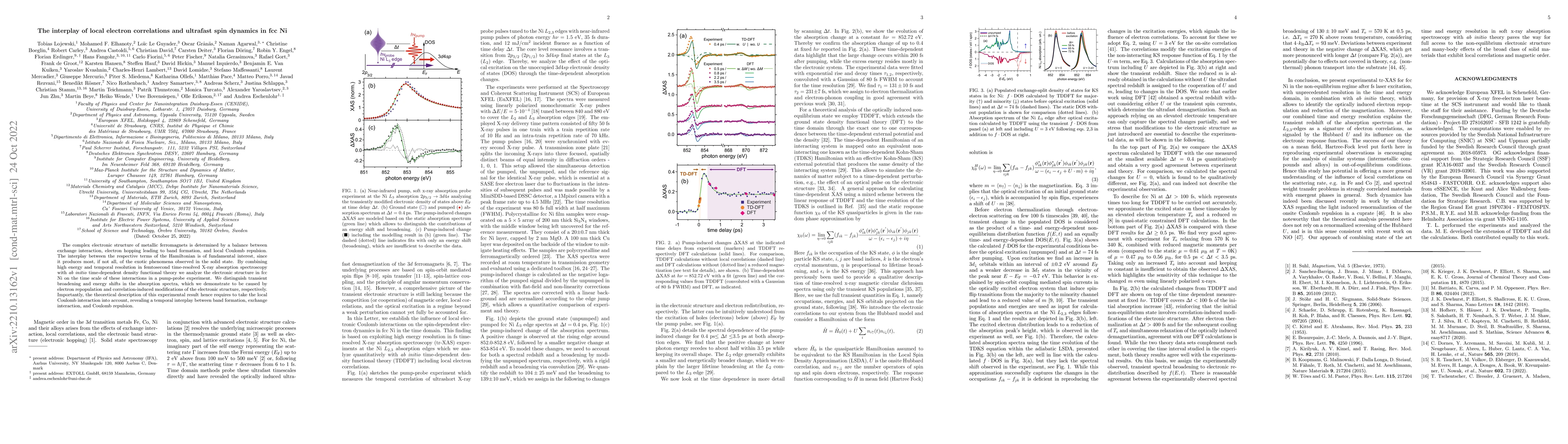
The complex electronic structure of metallic ferromagnets is determined by a balance between exchange interaction, electron hopping leading to band formation, and local Coulomb repulsion. The interp...
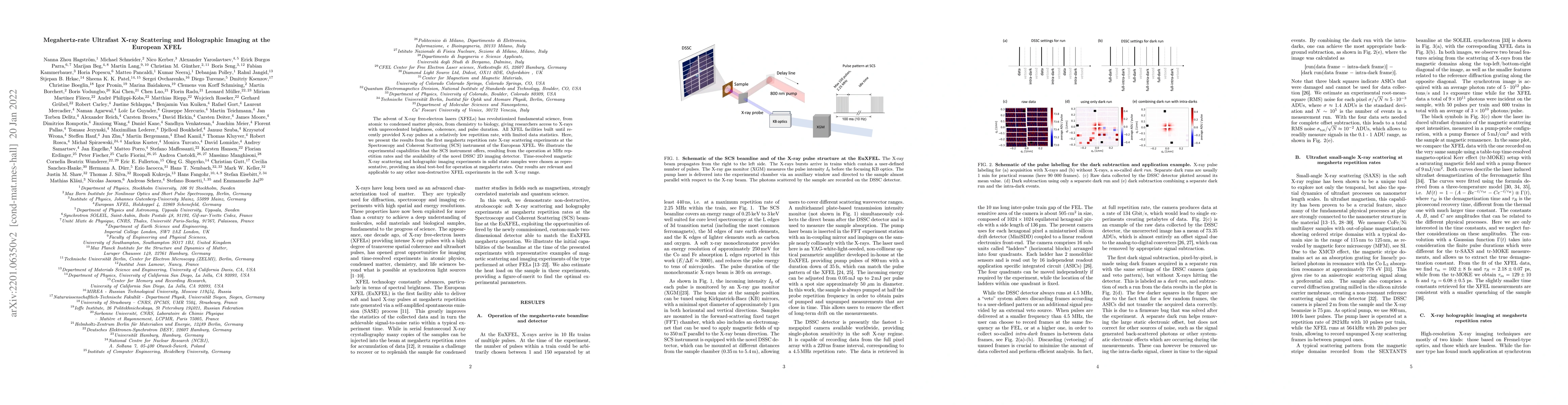
The advent of X-ray free-electron lasers (XFELs) has revolutionized fundamental science, from atomic to condensed matter physics, from chemistry to biology, giving researchers access to X-rays with ...
Time-resolved X-ray absorption spectroscopy (tr-XAS) has been shown to be a versatile measurement technique for investigating non-equilibrium dynamics. Novel X-ray free electron laser (XFEL) facilitie...
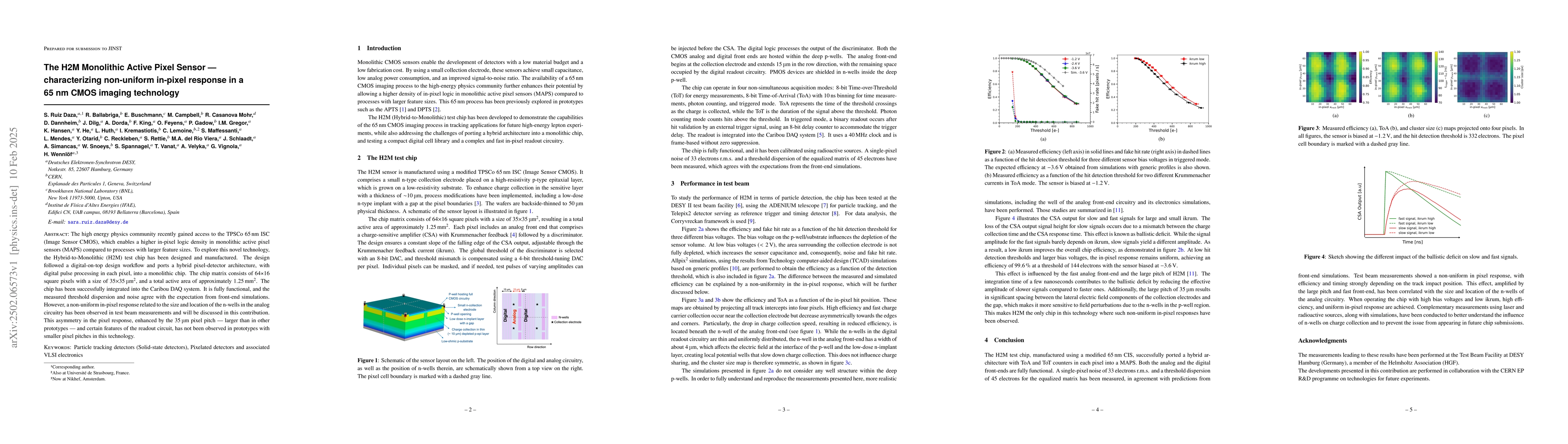
The high energy physics community recently gained access to the TPSCo 65 nm ISC (Image Sensor CMOS), which enables a higher in-pixel logic density in monolithic active pixel sensors (MAPS) compared to...
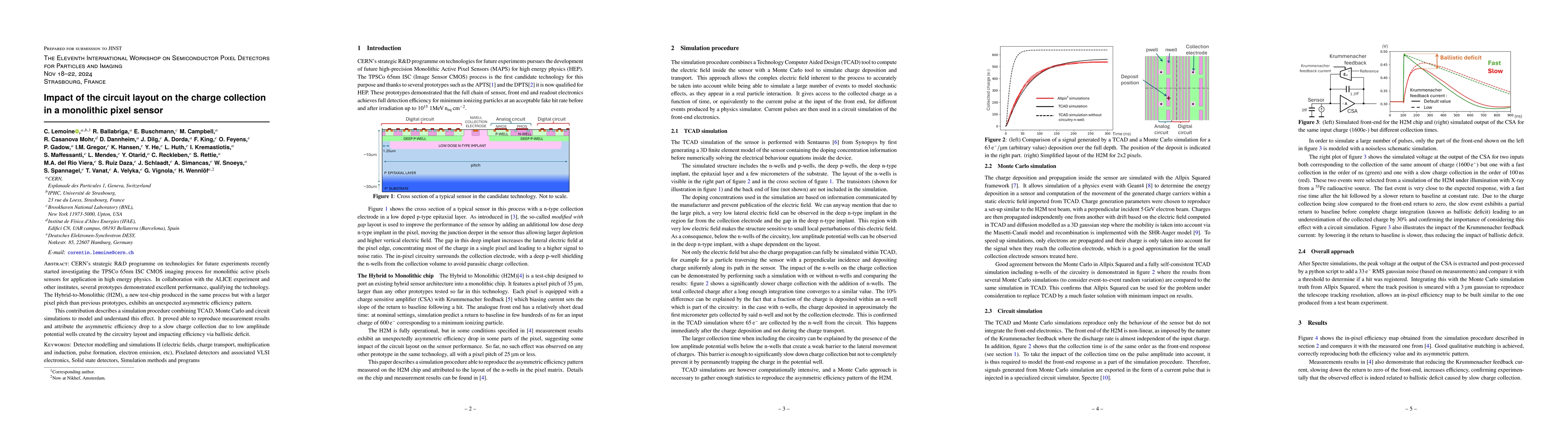
CERN's strategic R&D programme on technologies for future experiments recently started investigating the TPSCo 65nm ISC CMOS imaging process for monolithic active pixels sensors for application in hig...
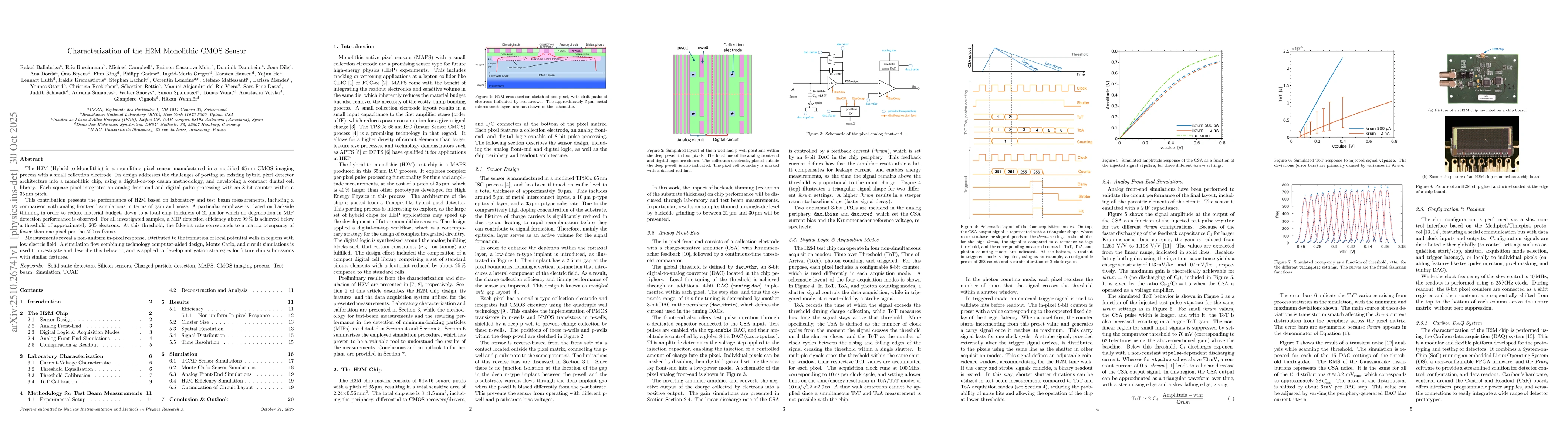
The H2M (Hybrid-to-Monolithic) is a monolithic pixel sensor manufactured in a modified \SI{65}{\nano\meter}~CMOS imaging process with a small collection electrode. Its design addresses the challenges ...