Academic Profile
Statistics
Similar Authors
Papers on arXiv
Nickel nanoparticles (Ni NPs), thanks to their peculiar properties, are interesting materials for many applications including catalysis, hydrogen storage, and sensors. In this work, Ni NPs are synth...
Atomically thin materials offer multiple opportunities for layer-by-layer control of their electronic properties. While monolayer graphene (MLG) is a zero-gap system, Bernal-stacked bilayer graphene...
Understanding and controlling the electronic properties of two-dimensional materials is crucial for their potential applications in nano- and optoelectronics. Monolayer transition metal dichalcogeni...
Two-dimensional (2D) materials have received extensive research attentions over the past two decades due to their intriguing physical properties (such as the ultrahigh mobility and strong light-matt...
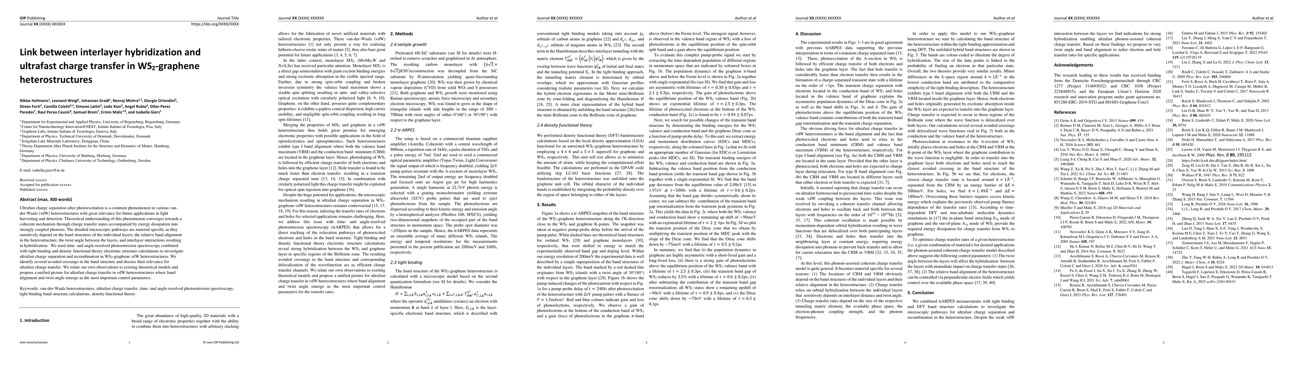
Ultrafast charge separation after photoexcitation is a common phenomenon in various van-der-Waals (vdW) heterostructures with great relevance for future applications in light harvesting and detectio...
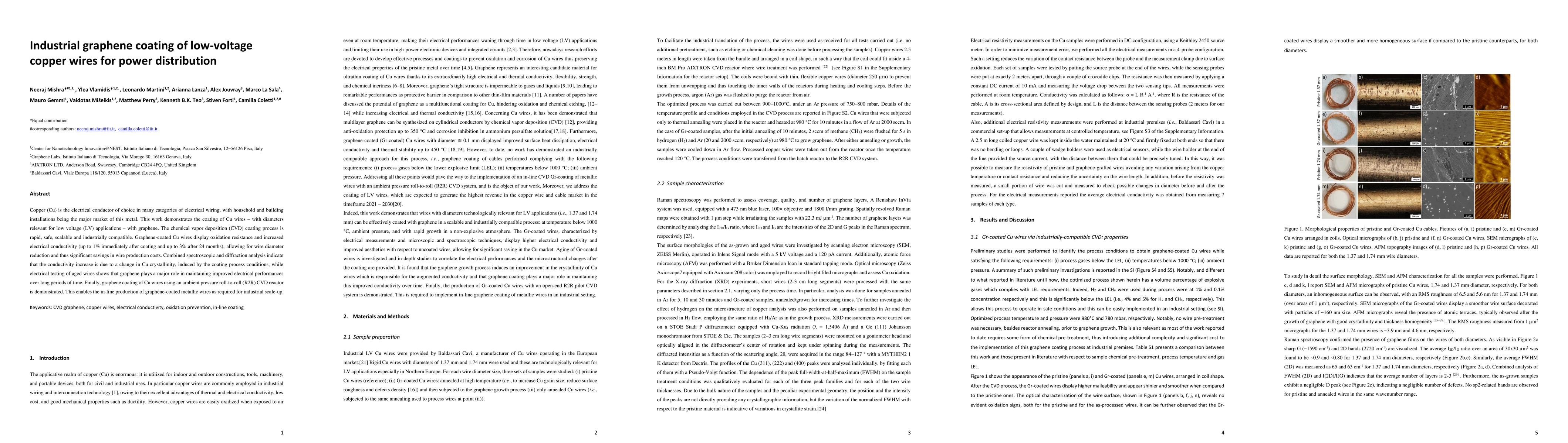
Copper (Cu) is the electrical conductor of choice in many categories of electrical wiring, with household and building installations being the major market of this metal. This work demonstrates the ...
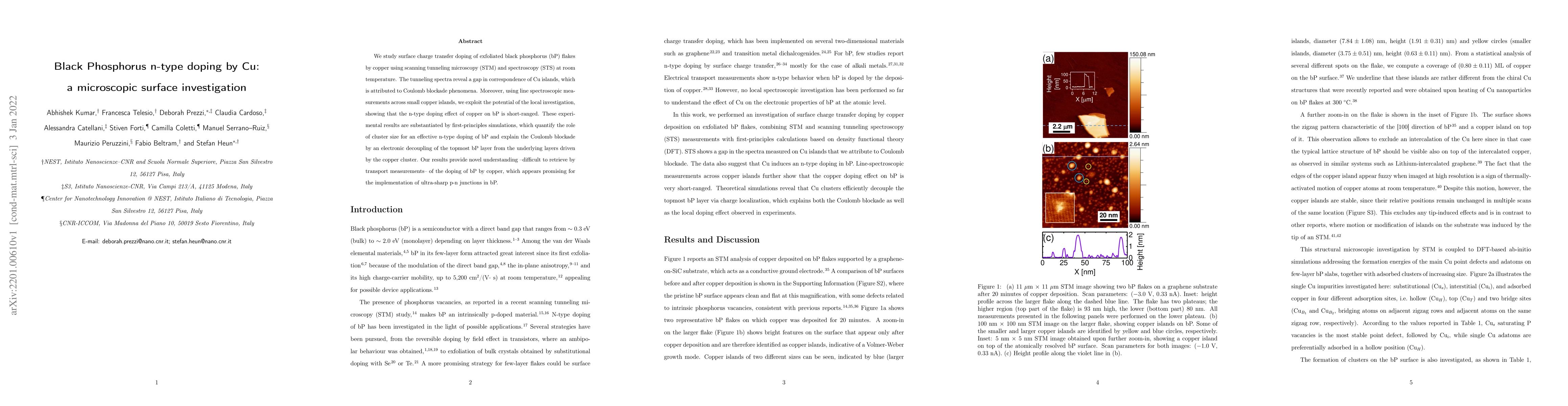
We study surface charge transfer doping of exfoliated black phosphorus (bP) flakes by copper using scanning tunneling microscopy (STM) and spectroscopy (STS) at room temperature. The tunneling spect...
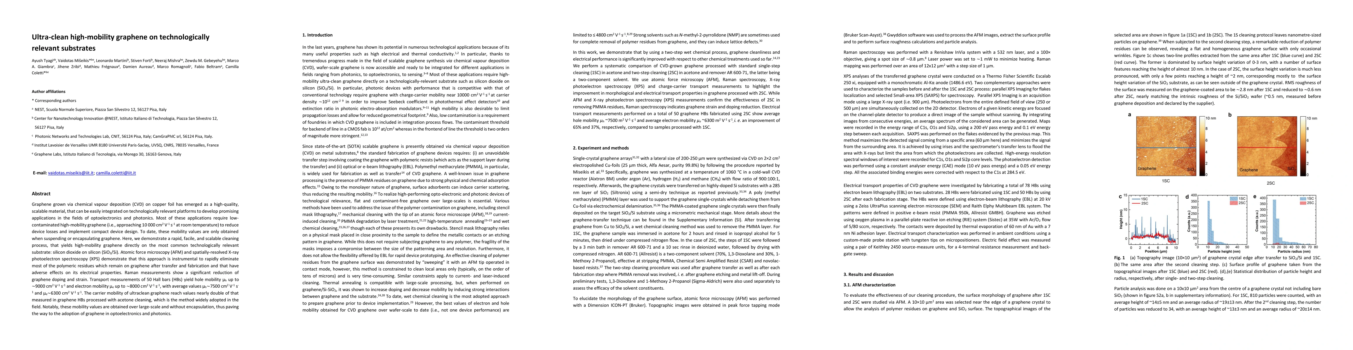
Graphene grown via chemical vapour deposition (CVD) on copper foil has emerged as a high-quality, scalable material, that can be easily integrated on technologically relevant platforms to develop pr...
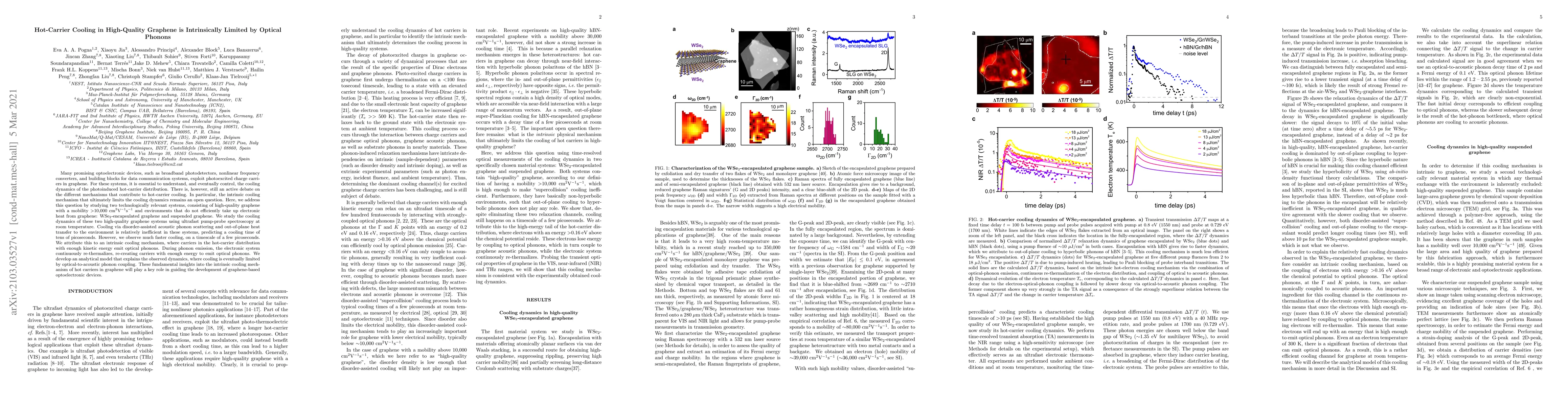
Many promising optoelectronic devices, such as broadband photodetectors, nonlinear frequency converters, and building blocks for data communication systems, exploit photoexcited charge carriers in g...
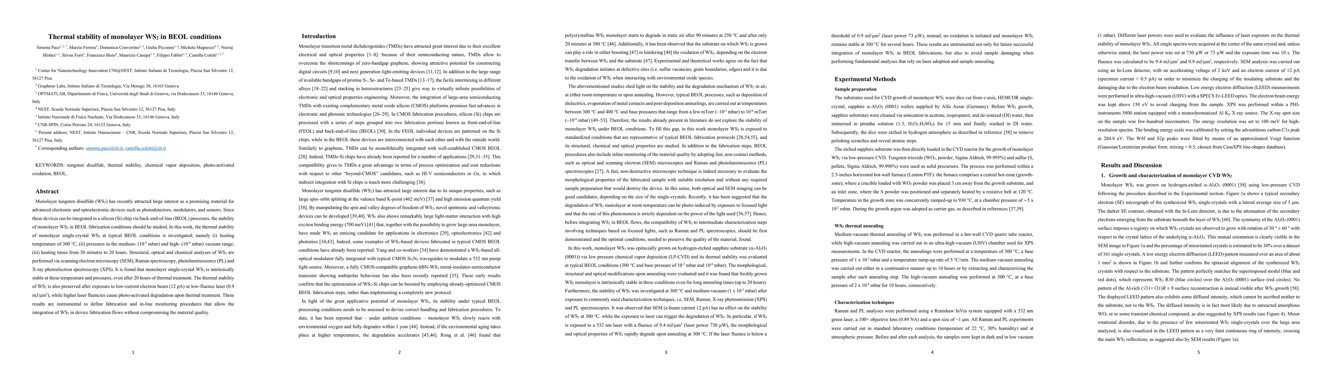
Monolayer tungsten disulfide ($WS_2$) has recently attracted large interest as a promising material for advanced electronic and optoelectronic devices such as photodetectors, modulators, and sensors...
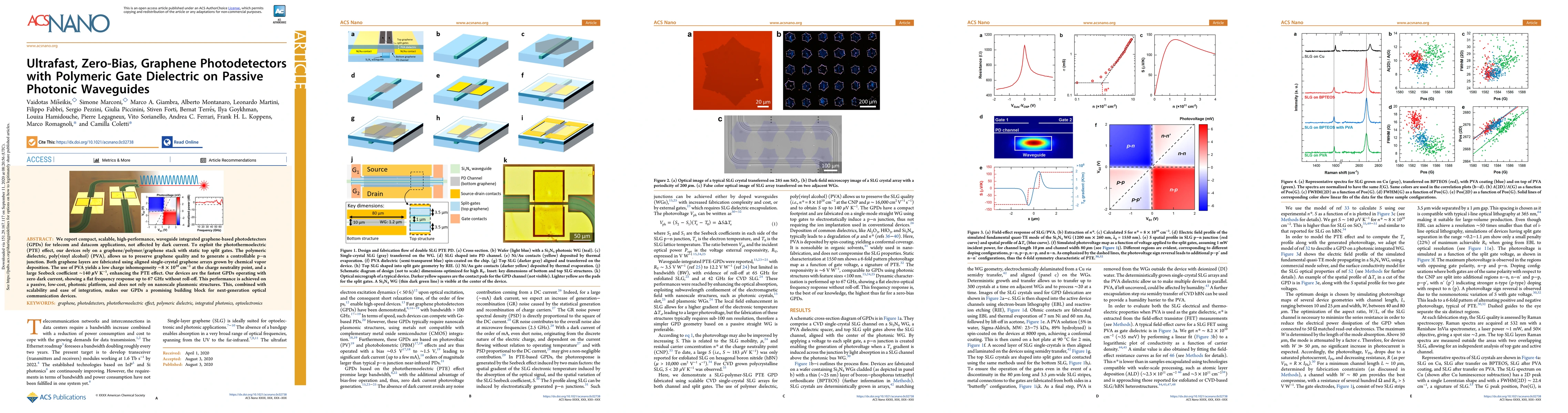
We report compact, scalable, high-performance, waveguide integrated graphene-based photodetectors (GPDs) for telecom and datacom applications, not affected by dark current. To exploit the phototherm...
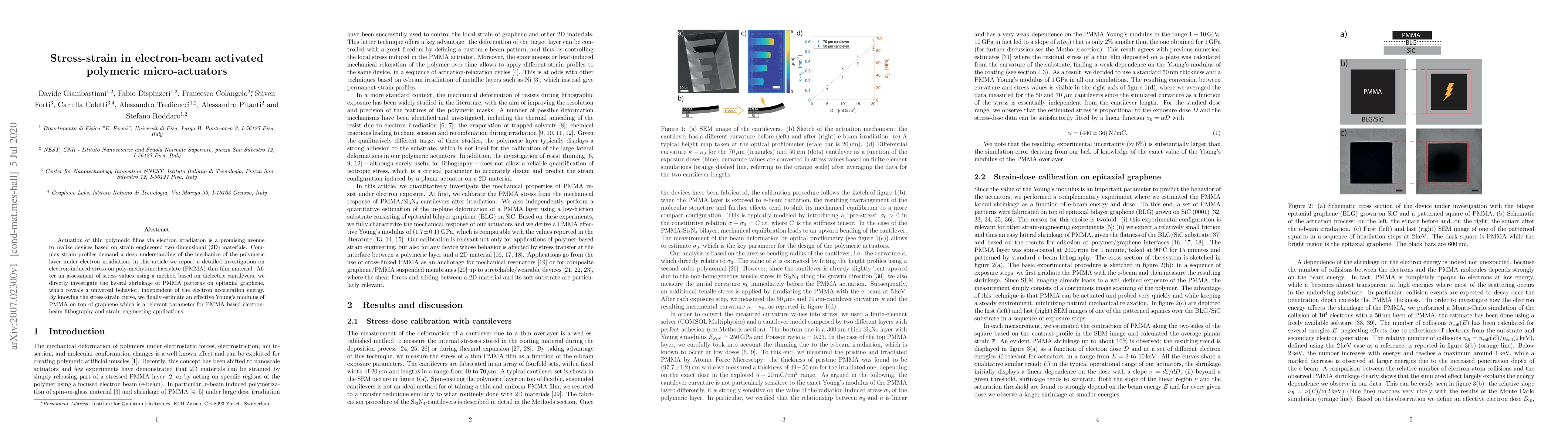
Actuation of thin polymeric films via electron irradiation is a promising avenue to realize devices based on strain engineered two dimensional (2D) materials. Complex strain profiles demand a deep u...
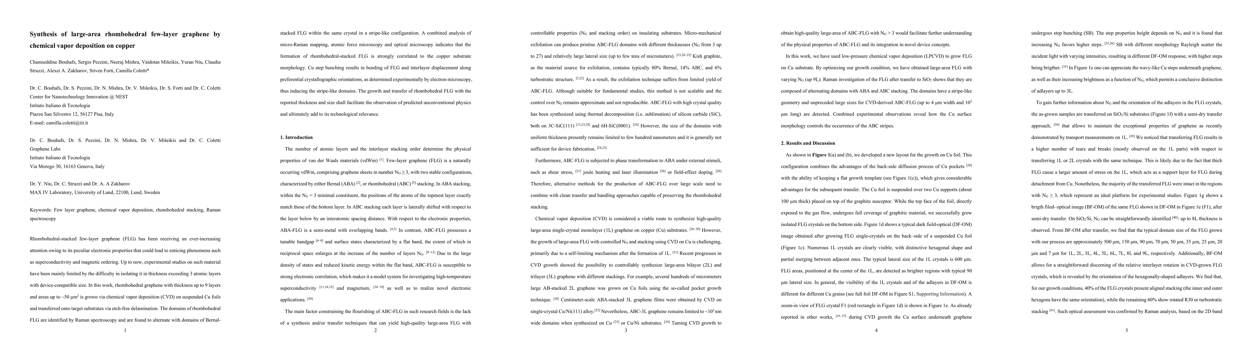
Rhombohedral-stacked few-layer graphene (FLG) has been receiving an ever-increasing attention owing to its peculiar electronic properties that could lead to enticing phenomena such as superconductiv...
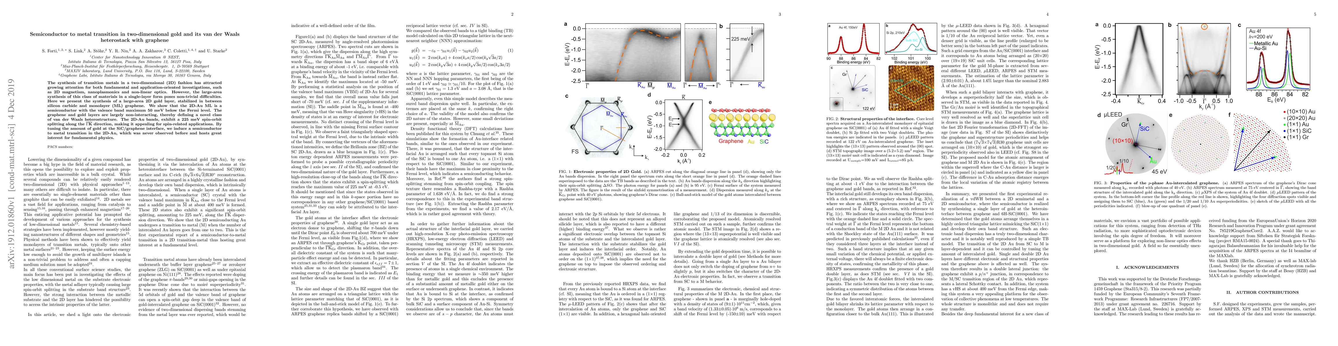
The synthesis of transition metals in a two-dimensional (2D) fashion has attracted growing attention for both fundamental and application-oriented investigations, such as 2D magnetism, nanoplasmonic...
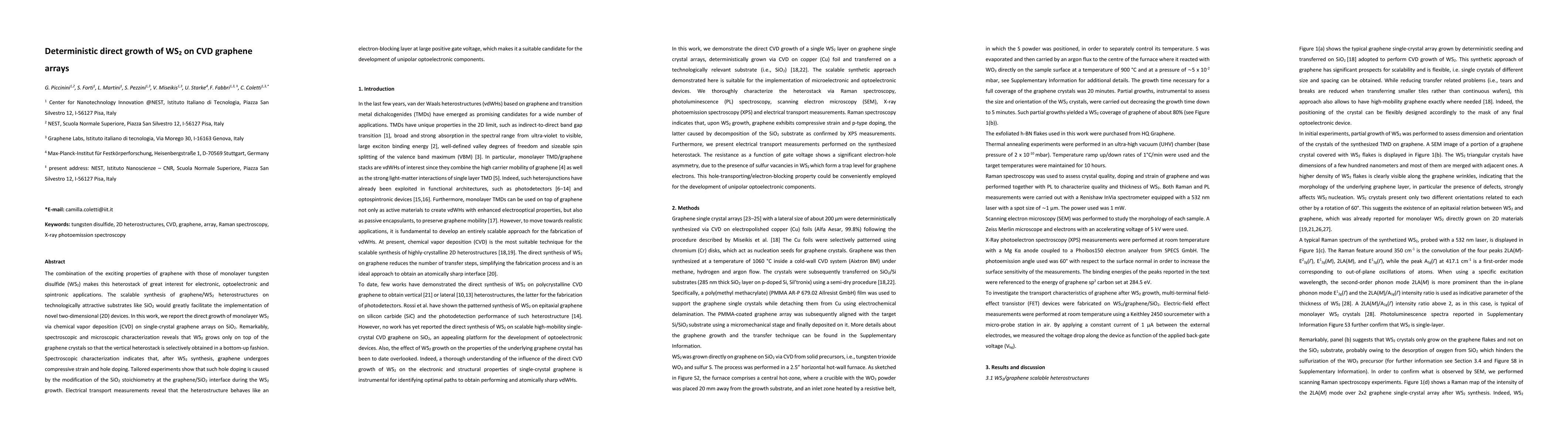
The combination of the exciting properties of graphene with those of monolayer tungsten disulfide (WS2) makes this heterostack of great interest for electronic, optoelectronic and spintronic applica...

Two-dimensional (2D) materials are poised to revolutionize current solid-state technology with their extraordinary properties. Yet, the primary challenge remains their scalable production. While there...
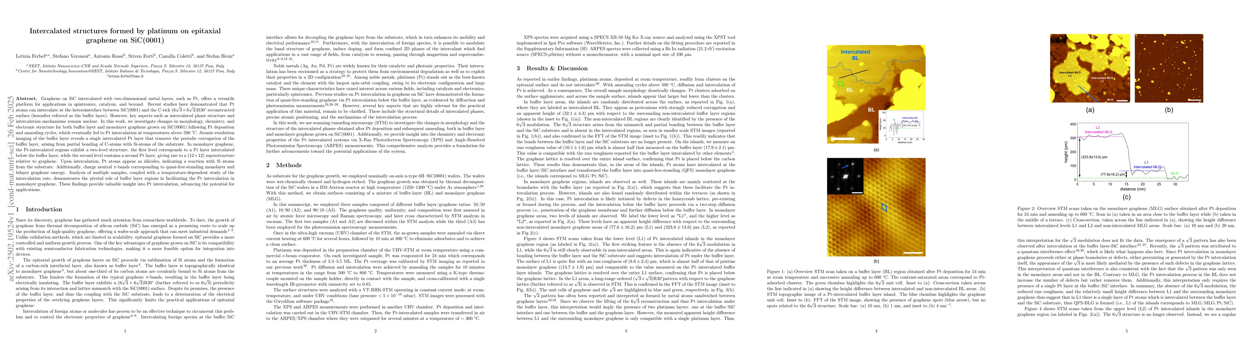
Graphene on SiC intercalated with two-dimensional metal layers, such as Pt, offers a versatile platform for applications in spintronics, catalysis, and beyond. Recent studies have demonstrated that Pt...
Efficient charge separation in van der Waals (vdW) heterostructures is crucial for optimizing light-harvesting and detection applications. However, precise control over the microscopic pathways govern...
Controlling doping is key to optimizing graphene for high-speed electronic and optoelectronic devices. However, its impact on non-equilibrium carrier lifetimes remains debated. Here, we systematically...
The creation of atomically thin layers of non-exfoliable materials remains a crucial challenge, requiring the development of innovative techniques. Here, confinement epitaxy is exploited to realize tw...
The electronic and vibrational properties of 2D materials are dramatically altered by the formation of a moiré superlattice. The lowest-energy phonon modes of the superlattice are two acoustic branche...
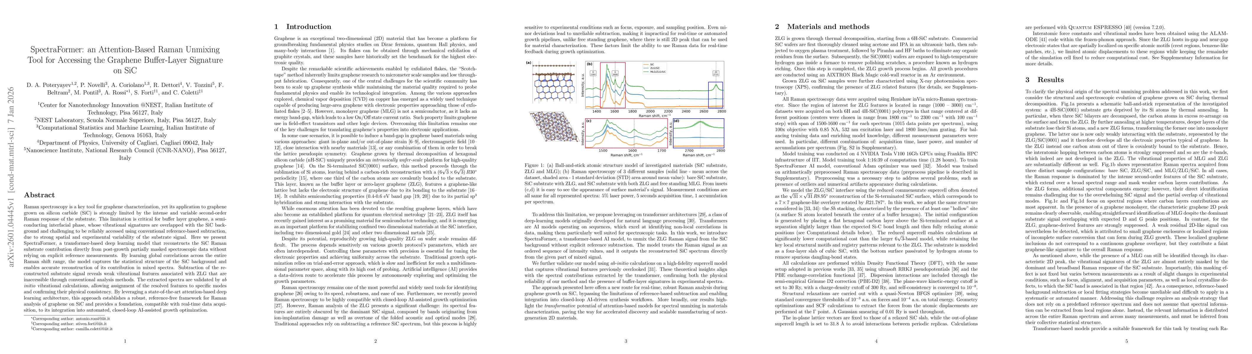
Raman spectroscopy is a key tool for graphene characterization, yet its application to graphene grown on silicon carbide (SiC) is strongly limited by the intense and variable second-order Raman respon...
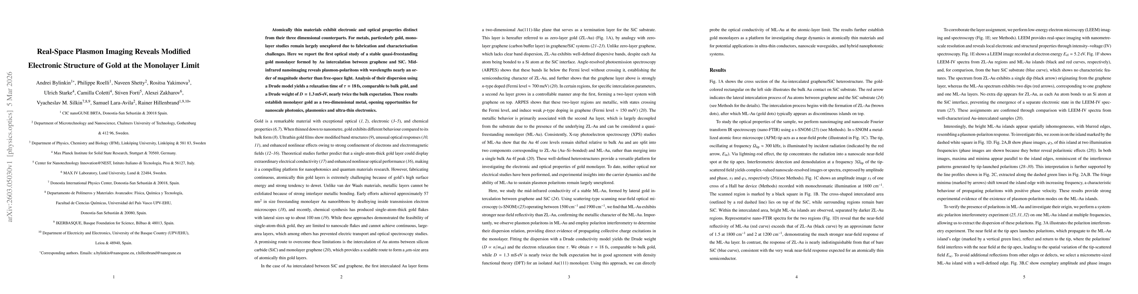
Atomically thin materials exhibit electronic and optical properties distinct from their three-dimensional counterparts. For metals, particularly gold, monolayer studies remain largely unexplored due t...
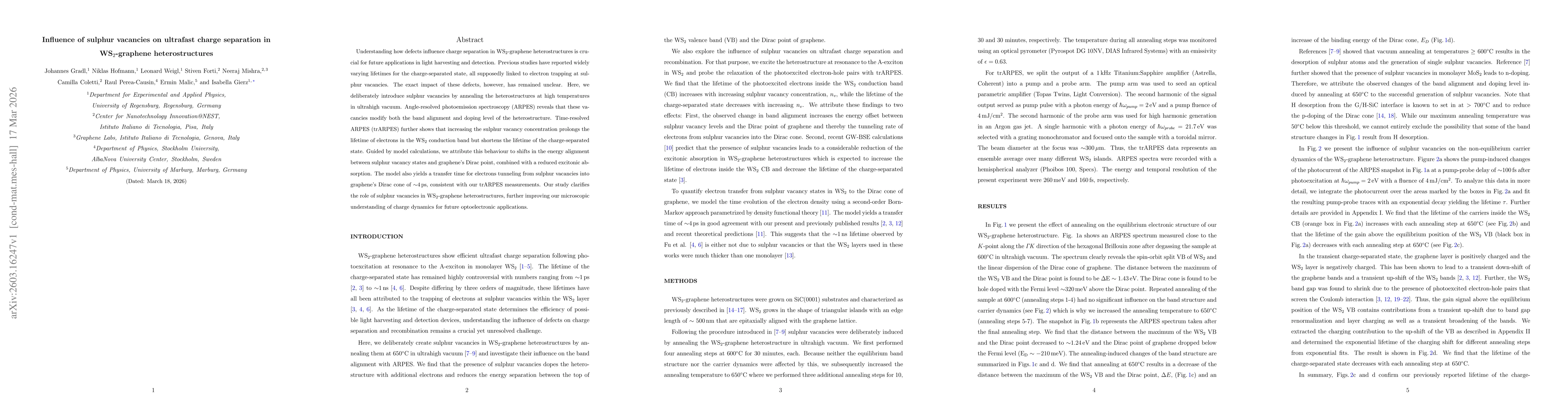
Understanding how defects influence charge separation in WS$_2$-graphene heterostructures is crucial for future applications in light harvesting and detection. Previous studies have reported widely va...

Two-dimensional (2D) magnetic materials integrated with graphene offer a compelling platform for next-generation spintronic devices, yet nickel in its 2D form remains largely unexplored, due to fundam...
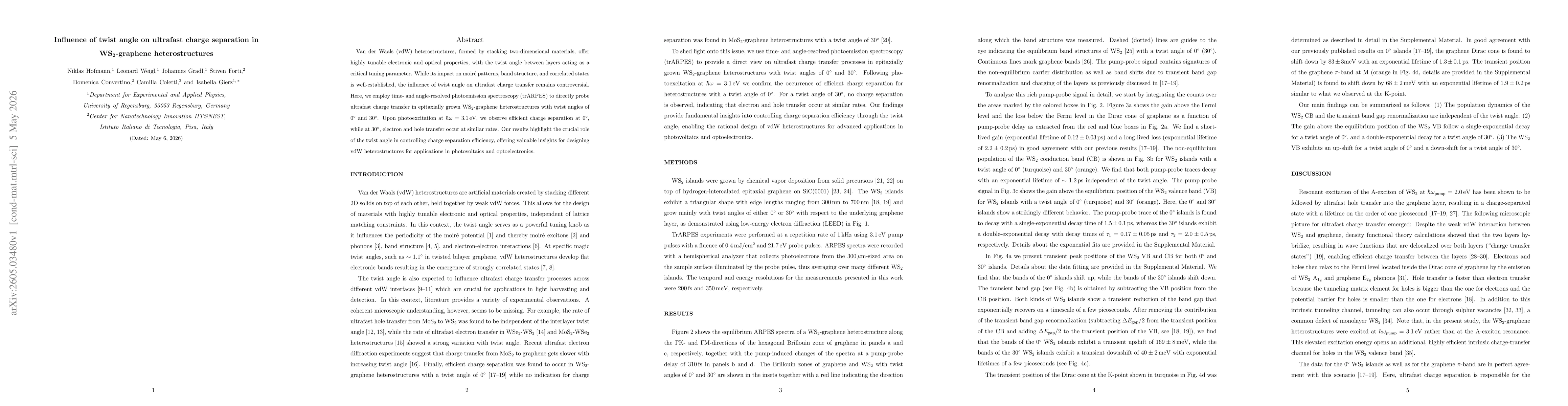
Van der Waals (vdW) heterostructures, formed by stacking two-dimensional materials, offer highly tunable electronic and optical properties, with the twist angle between layers acting as a critical tun...
Hybridization of highly itinerant Dirac electrons with localized flat-band states is predicted to yield emergent phenomena such as exotic heavy-fermion behaviour. Epitaxial graphene on two-dimensional...