ArxivLens
S
Researcher

Subhabrata Dhar

19 papers on arXiv

19 arXiv Papers
20 Total Publications
Profile

Academic Profile

Name S. Dhar
Total Papers 20
Scholar Profile View on Semantic Scholar
Metrics

Statistics

19 arXiv Papers
20 Total Publications
Publications

Papers on arXiv

Thumbnail for Influence of strain and point defects on the electronic structure and
  related properties of (111)NiO epitaxial films
arXiv
Influence of strain and point defects on the electronic structure and related properties of (111)NiO epitaxial films

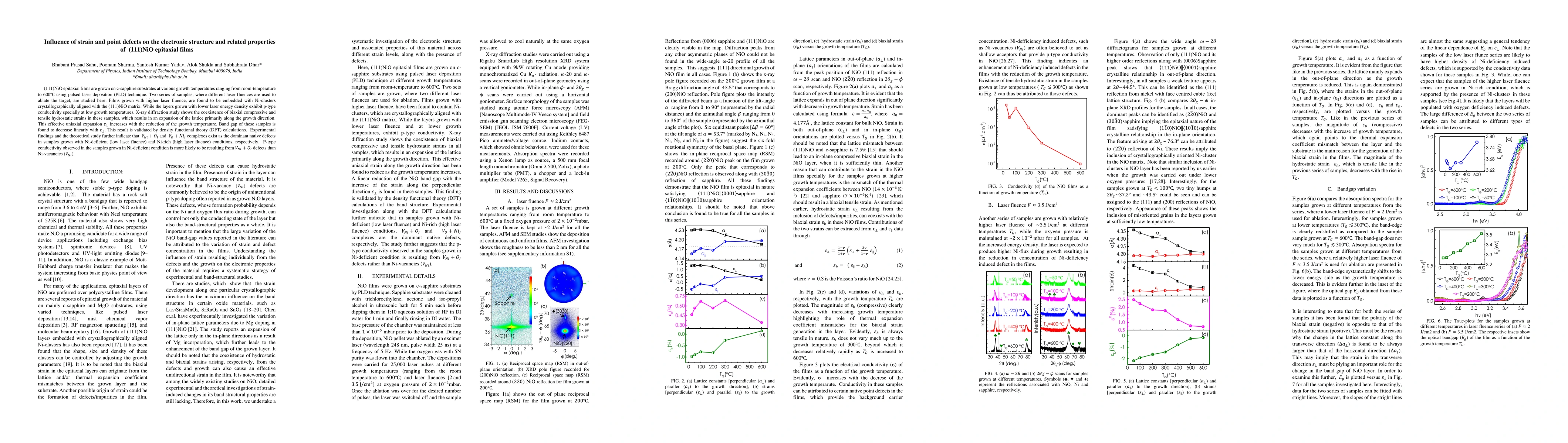
(111)NiO epitaxial films are grown on c-sapphire substrates at various growth temperatures ranging from room-temperature to 600C using pulsed laser deposition (PLD) technique. Two series of samples,...

Thumbnail for Ni cluster embedded (111)NiO layers grown on (0001)GaN films using
  pulsed laser deposition technique
arXiv
Ni cluster embedded (111)NiO layers grown on (0001)GaN films using pulsed laser deposition technique

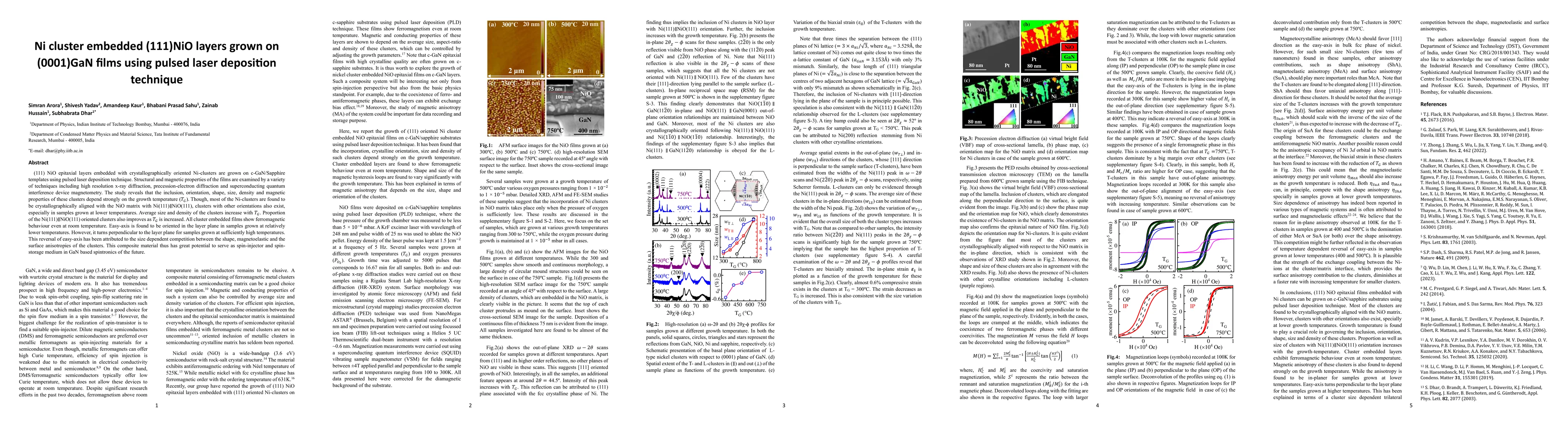
(111) NiO epitaxial layers embedded with crystallographically oriented Ni-clusters are grown on c-GaN/Sapphire templates using pulsed laser deposition technique. Structural and magnetic properties o...

Thumbnail for An electroplating-based plasmonic platform for giant emission
  enhancement in monolayer semiconductors
arXiv
An electroplating-based plasmonic platform for giant emission enhancement in monolayer semiconductors

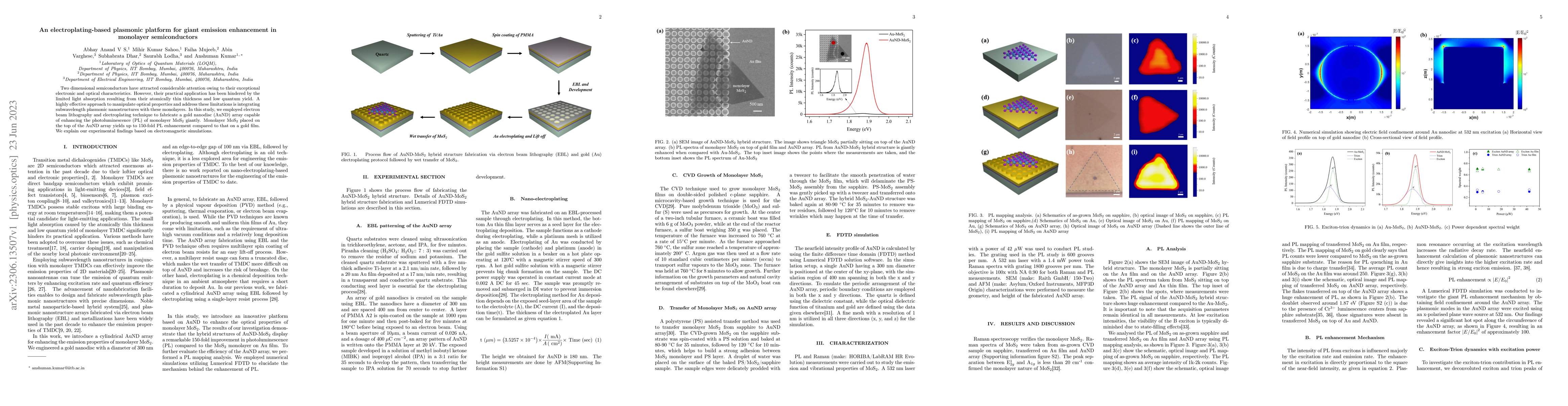
Two dimensional semiconductors have attracted considerable attention owing to their exceptional electronic and optical characteristics. However, their practical application has been hindered by the ...

Thumbnail for Spatially indirect interfacial excitons in n-ZnO/p-GaN heterostructures
arXiv
Spatially indirect interfacial excitons in n-ZnO/p-GaN heterostructures

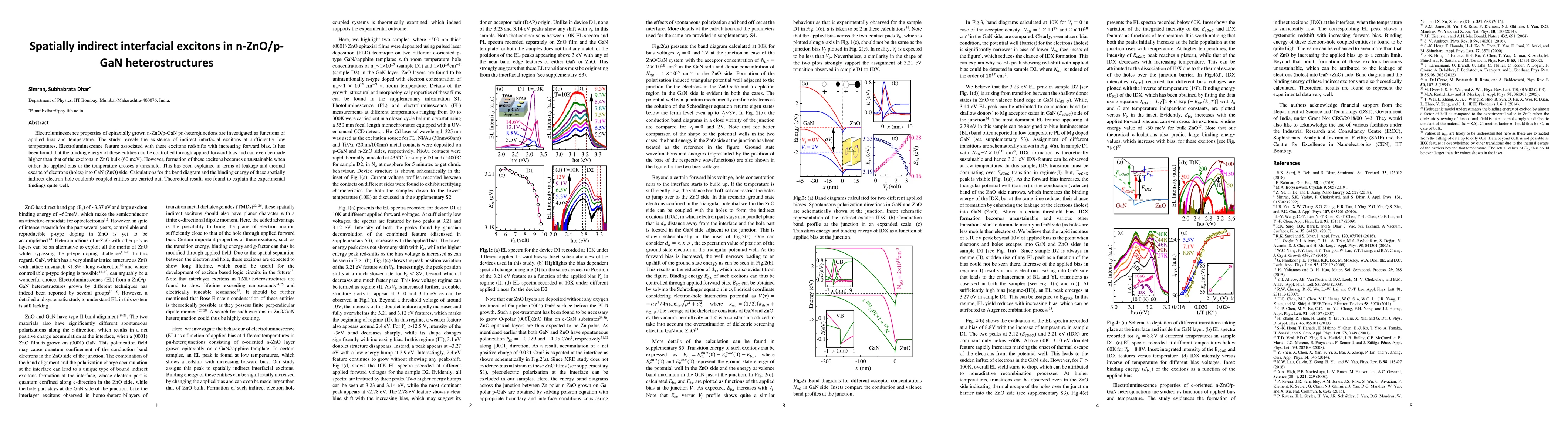
Electroluminescence properties of epitaxially grown n-ZnO/p-GaN pn-heterojunctions are investigated as functions of applied bias and temperature. The study reveals the existence of indirect interfac...

Thumbnail for Influence of Defects on the Valley Polarization Properties of Monolayer
  MoS$_{2}$ Grown by Chemical Vapor Deposition
arXiv
Influence of Defects on the Valley Polarization Properties of Monolayer MoS$_{2}$ Grown by Chemical Vapor Deposition

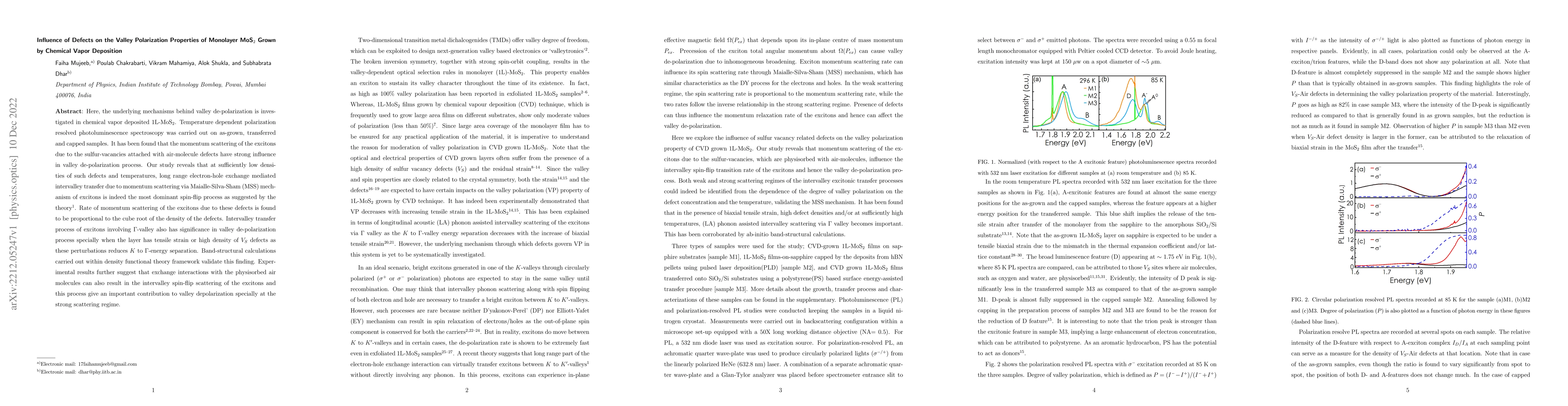
Here, the underlying mechanisms behind valley de-polarization is investigated in chemical vapor deposited 1L-MoS$_{2}$. Temperature dependent polarization resolved photoluminescence spectroscopy was...

Thumbnail for Effect of strain and sulfur vacancies on the luminescence and valley
  polarization properties of CVD grown monolayer MoS$_2$ films
arXiv
Effect of strain and sulfur vacancies on the luminescence and valley polarization properties of CVD grown monolayer MoS$_2$ films

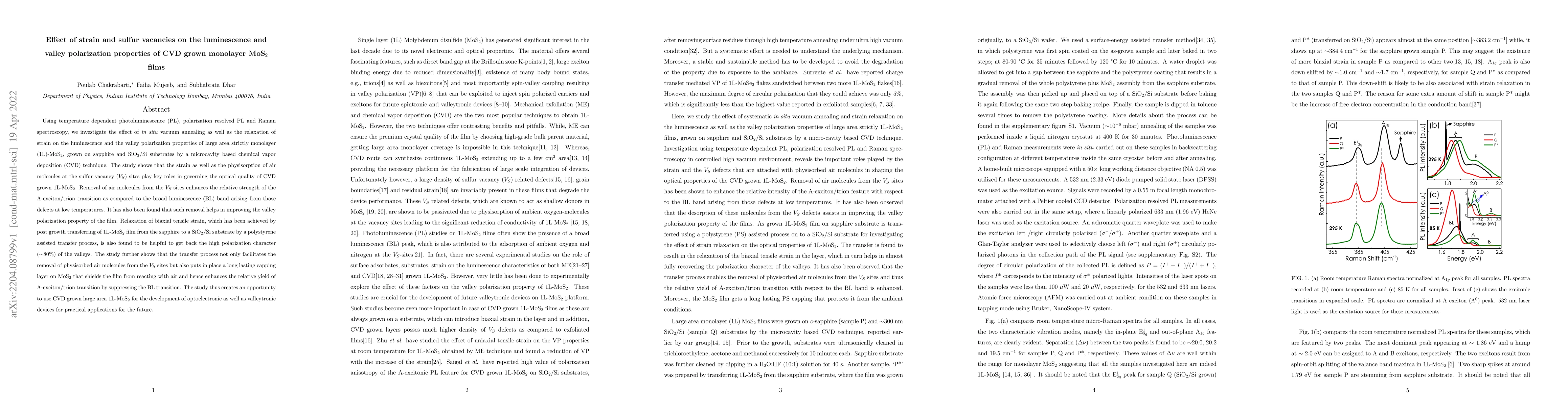
Using temperature dependent photoluminescence (PL), polarization resolved PL and Raman spectroscopy, we investigate the effect of in situ vacuum annealing as well as the relaxation of strain on the ...

Thumbnail for Effect of manganese incorporation on the excitonic recombination
  dynamics in monolayer MoS$_2$
arXiv
Effect of manganese incorporation on the excitonic recombination dynamics in monolayer MoS$_2$

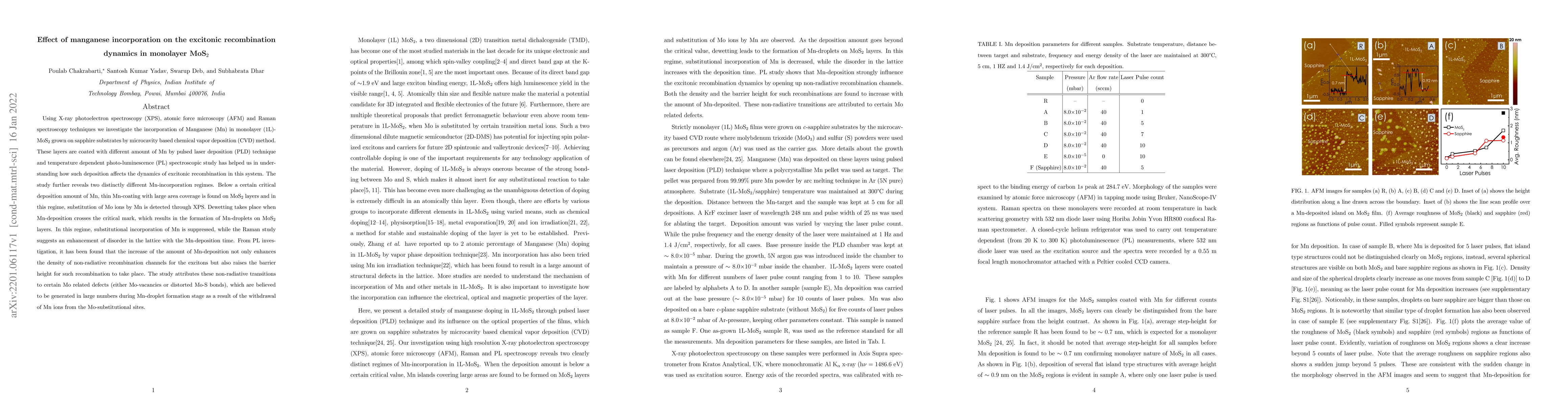
Using X-ray photoelectron spectroscopy (XPS), atomic force microscopy (AFM) and Raman spectroscopy techniques we investigate the incorporation of Manganese (Mn) in monolayer (1L)-MoS$_2$ grown on sa...

Thumbnail for Very thin (111) NiO epitaxial films grown on c-sapphire substrates by
  pulsed laser deposition technique
arXiv
Very thin (111) NiO epitaxial films grown on c-sapphire substrates by pulsed laser deposition technique

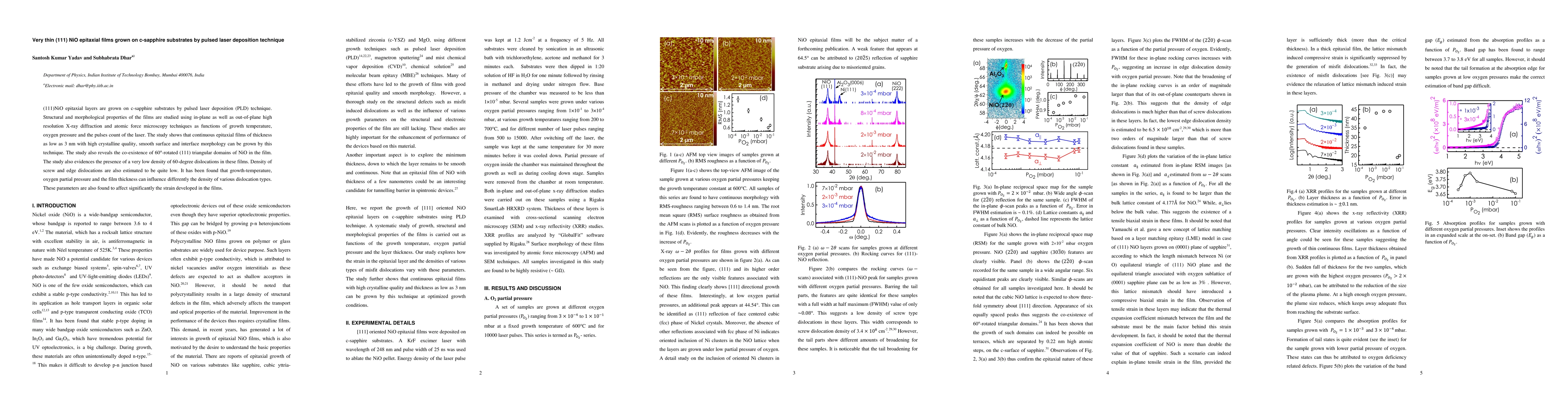
(111)NiO epitaxial layers are grown on c-sapphire substrates by pulsed laser deposition (PLD) technique. Structural and morphological properties of the films are studied using in-plane as well as ou...

Thumbnail for Spin transport in polarization induced two dimensional confinement of
  carriers in wedge shaped \textit{c}-GaN nanowalls
arXiv
Spin transport in polarization induced two dimensional confinement of carriers in wedge shaped \textit{c}-GaN nanowalls

Spin transport property of polarization induced two-dimensional electron gas channel formed in the central vertical plane of a wedge-shaped \textit{c}-oriented GaN nanowall is investigated theoretic...

Thumbnail for Tunability of electrical and thermoelectrical properties of monolayer
  MoS$_2$ through oxygen passivation
arXiv
Tunability of electrical and thermoelectrical properties of monolayer MoS$_2$ through oxygen passivation

Electric and thermoelectric properties of strictly monolayer MoS$_2$ films, which are grown using a novel micro-cavity based CVD growth technique, have been studied under diverse environmental and a...

Thumbnail for Controlled Growth of large area bilayer MoS$_2$ films on SiO$_2$
  substrates by chemical vapour deposition technique
arXiv
Controlled Growth of large area bilayer MoS$_2$ films on SiO$_2$ substrates by chemical vapour deposition technique

Bilayer (2L) transition metal dichalcogenides (TMD) have the ability to host interlayer excitons, where electron and hole parts are spatially separated that leads to much longer lifetime as compared t...

Thumbnail for p-(001)NiO/n-(0001)ZnO heterostructures grown by pulsed laser deposition
  technique
arXiv
p-(001)NiO/n-(0001)ZnO heterostructures grown by pulsed laser deposition technique

NiO/ZnO heterostructures are grown on c-sapphire substrates using pulsed laser deposition (PLD) technique. X-ray diffraction study shows that the ZnO layer epitaxially grows along [0001]-direction on ...

Thumbnail for p-(001)NiO/n-(0001)ZnO Heterostructures based Ultraviolet Photodetectors
arXiv
p-(001)NiO/n-(0001)ZnO Heterostructures based Ultraviolet Photodetectors

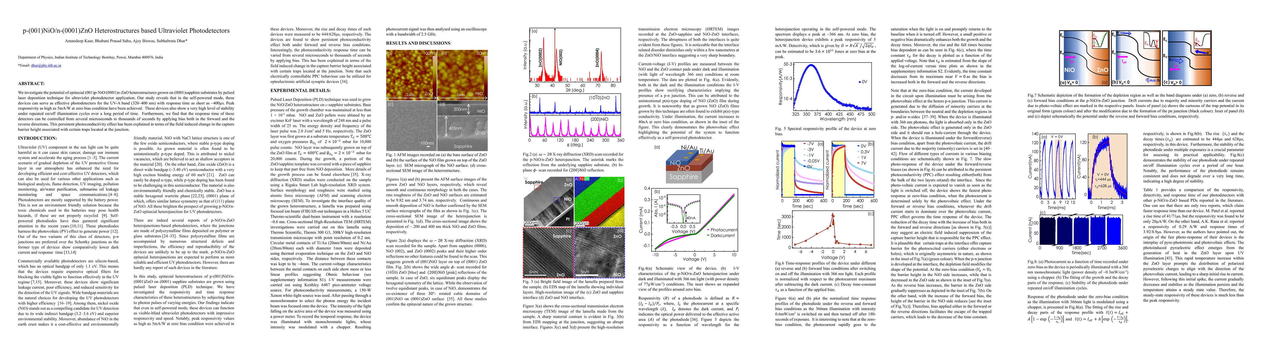
We investigate the potential of epitaxial (001)p-NiO/(0001)n-ZnO heterostructures grown on (0001)sapphire substrates by pulsed laser deposition technique for ultraviolet photodetector application. Our...

Thumbnail for Experimental demonstration of two distinct pathways of trion generation
  in monolayer MoS2
arXiv
Experimental demonstration of two distinct pathways of trion generation in monolayer MoS2

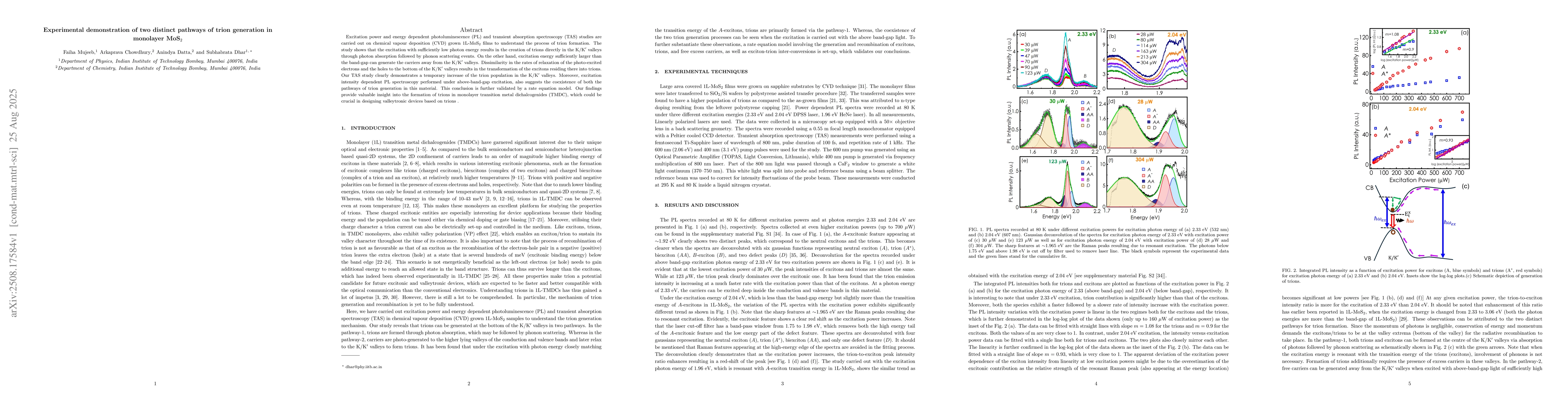
Excitation power and energy dependent photoluminescence (PL) and transient absorption spectroscopy (TAS) studies are carried out on chemical vapour deposition (CVD) grown 1L-MoS2 films to understand t...

Thumbnail for High-energy electron-beam induced defect engineering of monolayer MoS2
  for tunable optical properties
arXiv
High-energy electron-beam induced defect engineering of monolayer MoS2 for tunable optical properties

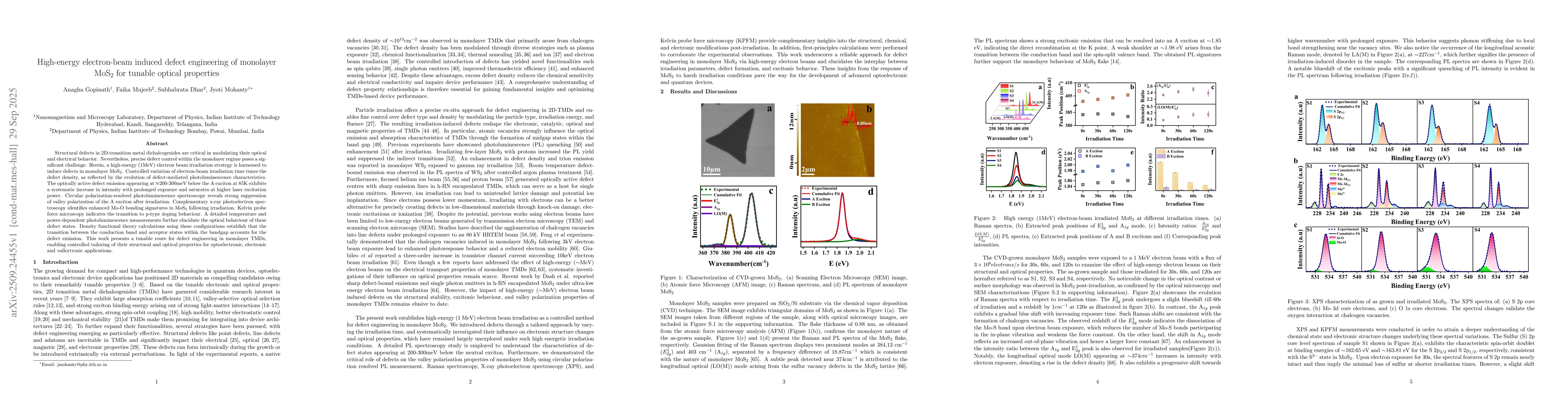
Structural defects in 2D-transition metal dichalcogenides are critical in modulating their optical and electrical behavior. Nevertheless, precise defect control within the monolayer regime poses a sig...

Thumbnail for Spontaneous growth of perfectly circular domains of MoS2 monolayers using chemical vapour deposition technique
arXiv
Spontaneous growth of perfectly circular domains of MoS2 monolayers using chemical vapour deposition technique

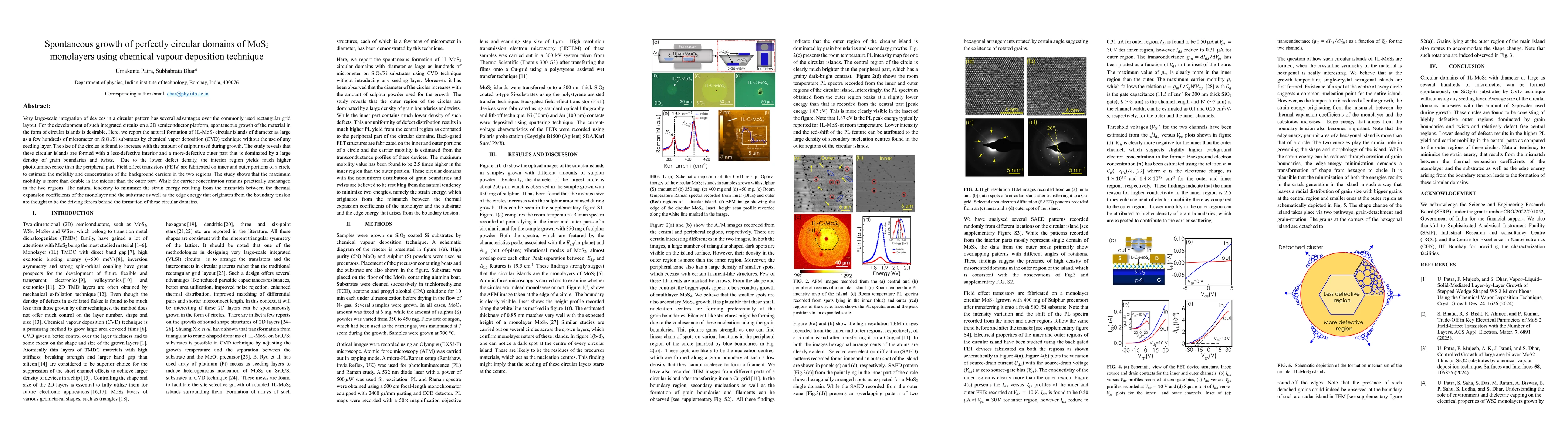
Very large-scale integration of devices in a circular pattern has several advantages over the commonly used rectangular grid layout. For the development of such integrated circuits on a 2D semiconduct...

Thumbnail for CVD grown bilayer MoS2 based artificial optoelectronic synapses for arithmetic computing and image recognition applications
arXiv
CVD grown bilayer MoS2 based artificial optoelectronic synapses for arithmetic computing and image recognition applications

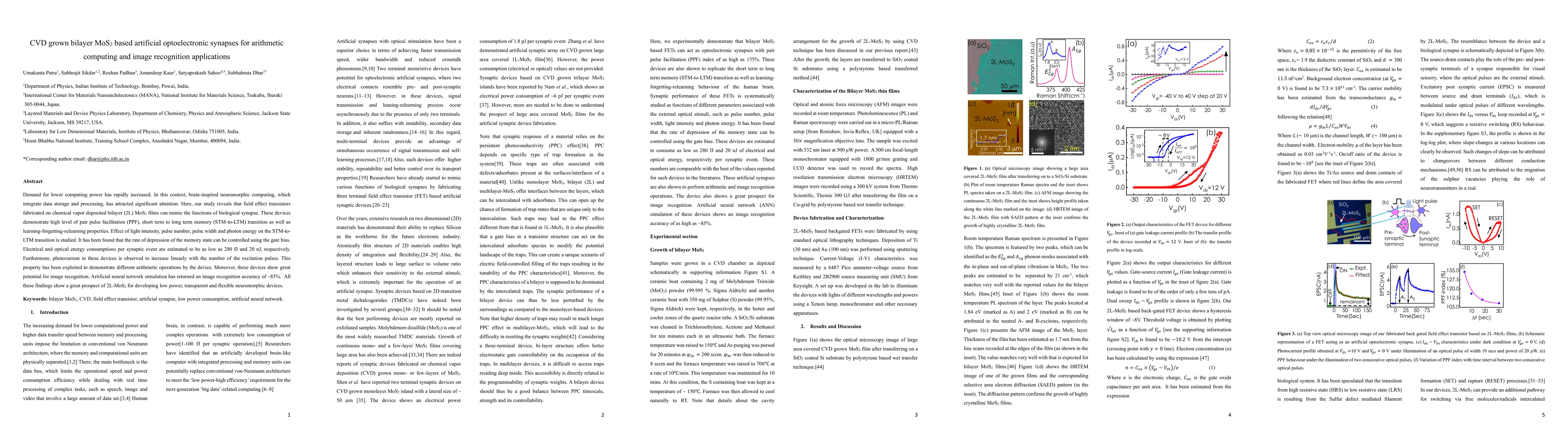
Demand for lower computing power has rapidly increased. In this context, brain-inspired neuromorphic computing, which integrate data storage and processing, has attracted significant attention. Here, ...

Thumbnail for Si-Ga2O3/p-GaN epitaxial heterostructure based self-powered and visible-blind UV photodetectors with fast and electrically tuneable response time
arXiv
Si-Ga2O3/p-GaN epitaxial heterostructure based self-powered and visible-blind UV photodetectors with fast and electrically tuneable response time

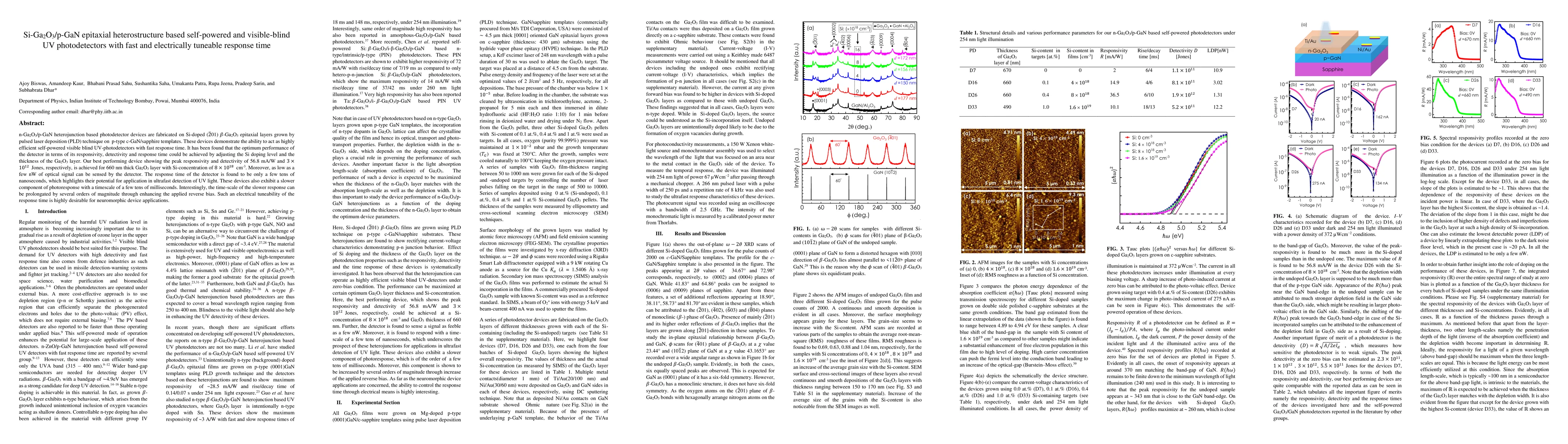
n-Ga2O3/p-GaN heterojunction based photodetector devices are fabricated on Si-doped (-201) β-Ga2O3 epitaxial layers grown by pulsed laser deposition (PLD) technique on p-type c-GaN/sapphire templates....

Thumbnail for Nanoscale mapping of stacking-dependent work function and local photoresponse in CVD-grown MoS2 bilayers by KPFM
arXiv
Nanoscale mapping of stacking-dependent work function and local photoresponse in CVD-grown MoS2 bilayers by KPFM

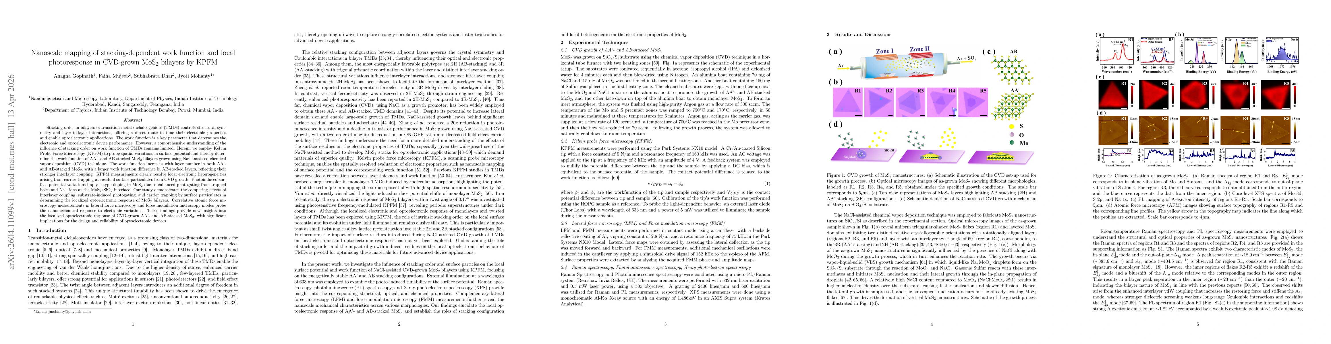
Stacking order in bilayers of transition metal dichalcogenides (TMDs) controls structural symmetry and layer-to-layer interactions, offering a direct route to tune their electronic properties and enab...

This website uses cookies to ensure you get the best experience. Learn more