Academic Profile
Statistics
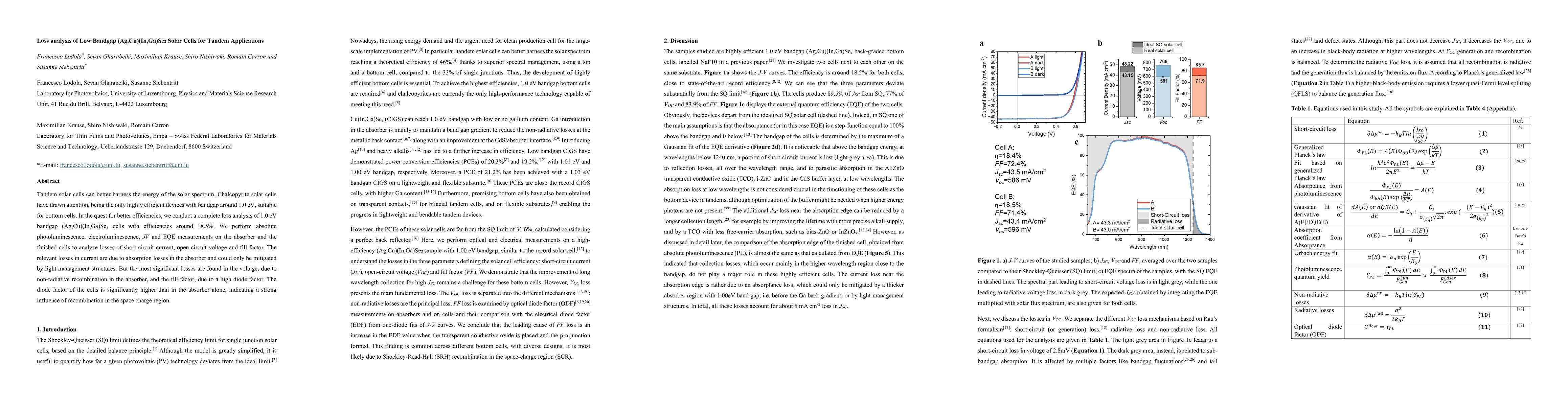
Similar Authors
Papers on arXiv
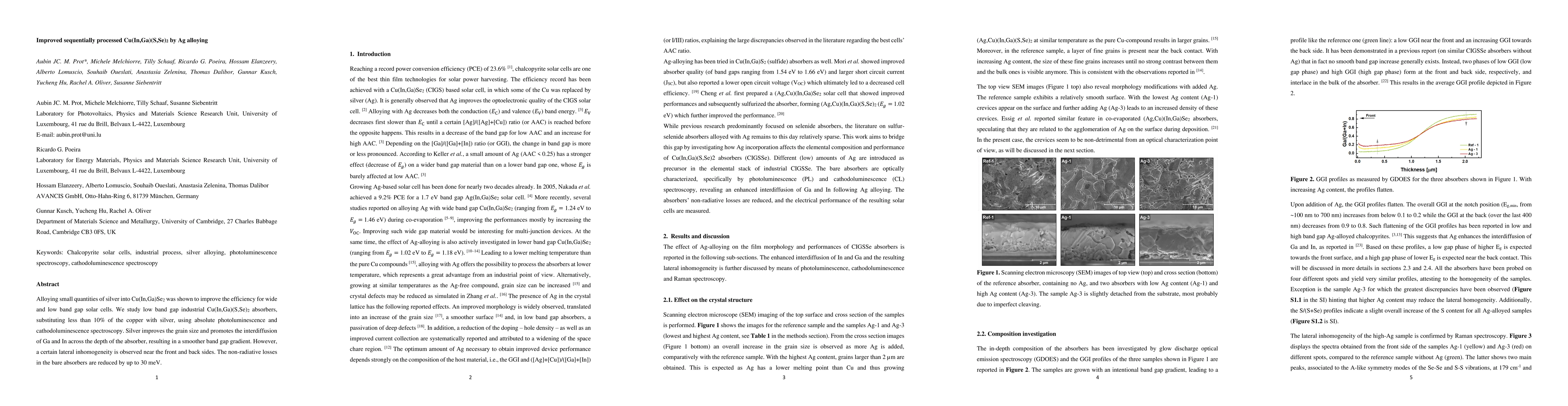
Alloying small quantities of silver into Cu(In,Ga)Se2 was shown to improve the efficiency for wide and low band gap solar cells. We study low band gap industrial Cu(In,Ga)(S,Se)2 absorbers, substitu...
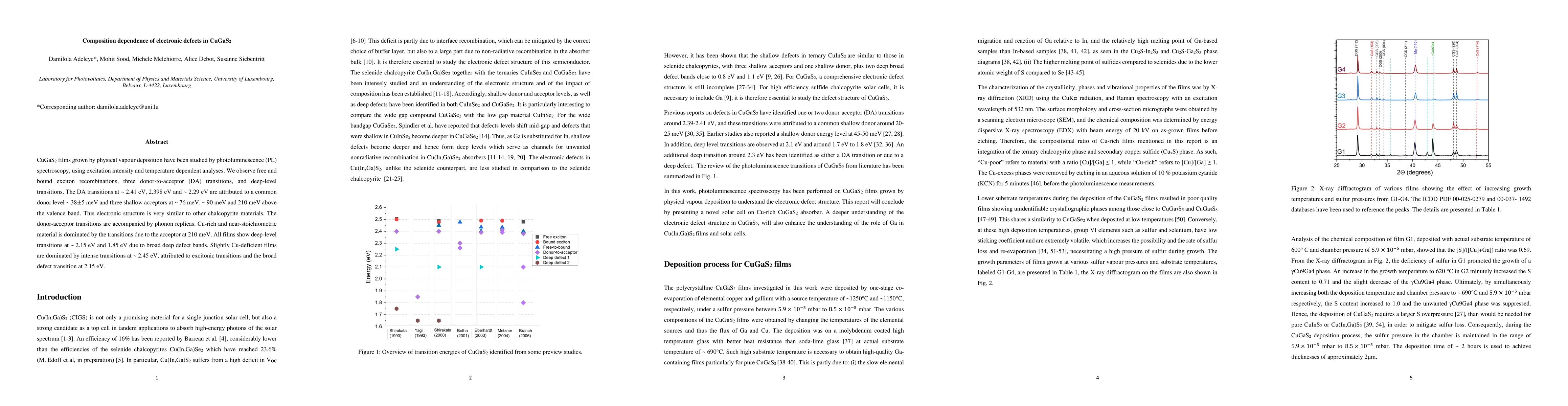
CuGaS2 films grown by physical vapour deposition have been studied by photoluminescence (PL) spectroscopy, using excitation intensity and temperature dependent analyses. We observe free and bound ex...
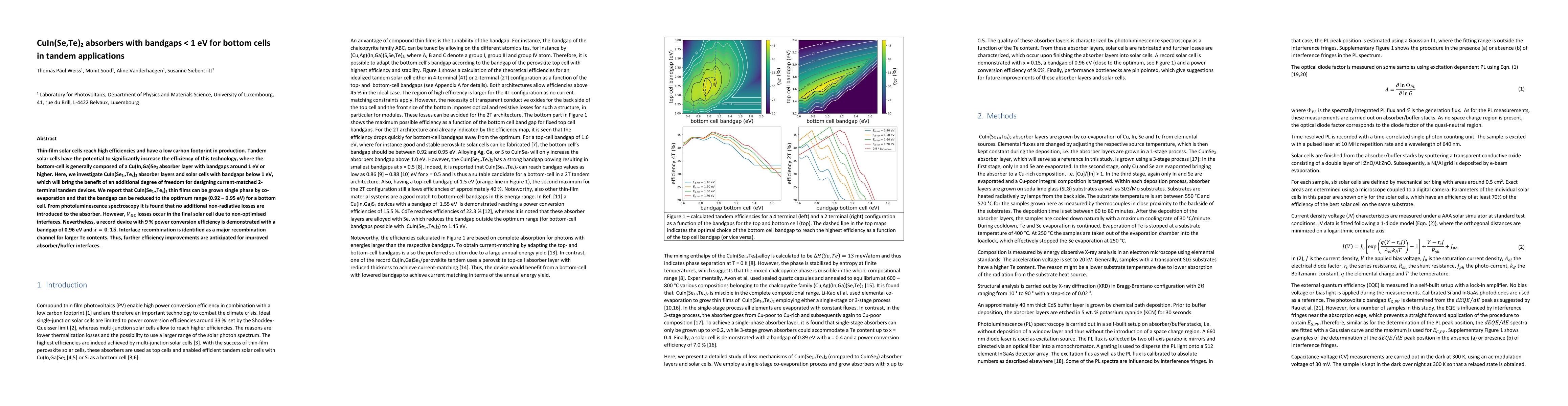
Thin-film solar cells reach high efficiencies and have a low carbon footprint in production. Tandem solar cells have the potential to significantly increase the efficiency of this technology, where ...
Record efficiency in chalcopyrite-based solar cells Cu(In,Ga)(S,Se)2 is achieved using a gallium gradient to increase the band gap of the absorber towards the back side. Although this structure has ...
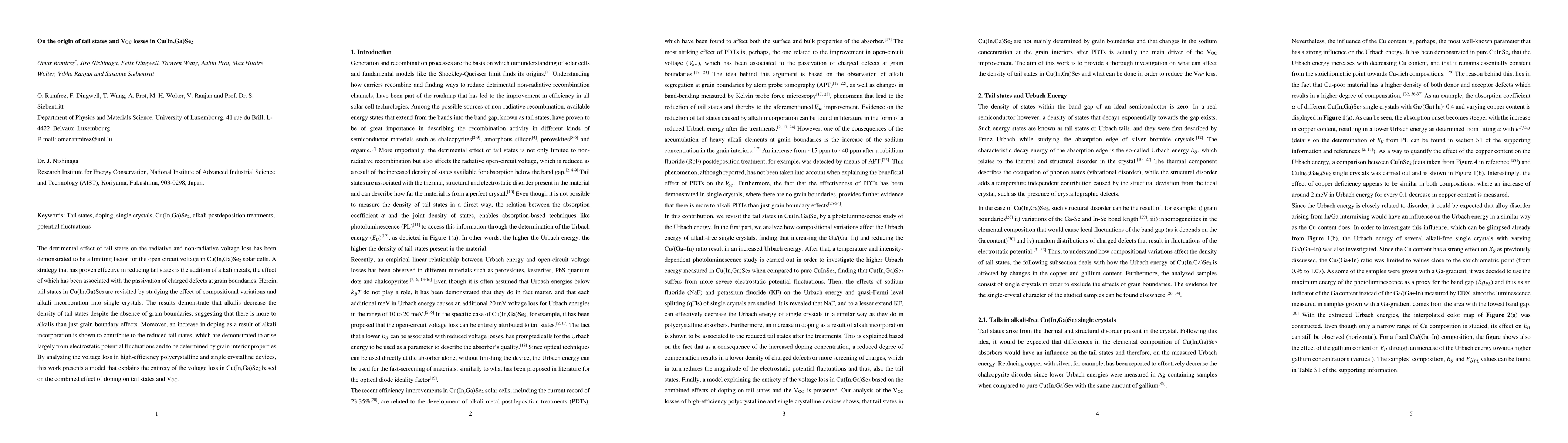
The detrimental effect of tail states on the radiative and non-radiative voltage loss has been demonstrated to be a limiting factor for the open circuit voltage in Cu(In,Ga)Se2 solar cells. A strate...
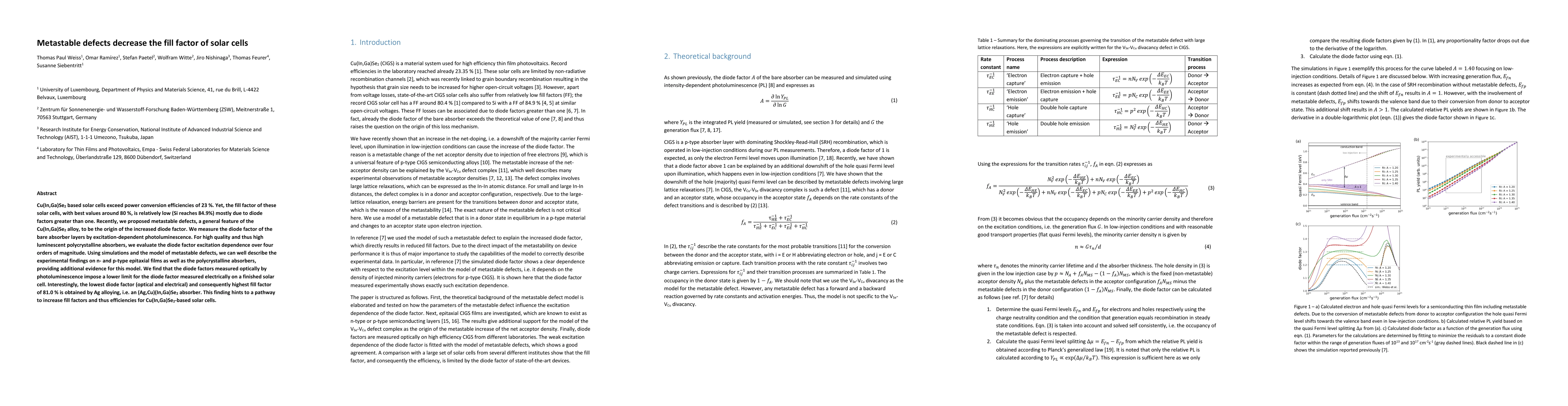
Cu(In,Ga)Se2 based solar cells exceed power conversion efficiencies of 23 %. Yet, the fill factor of these solar cells, with best values around 80 %, is relatively low (Si reaches 84.9%) mostly due ...
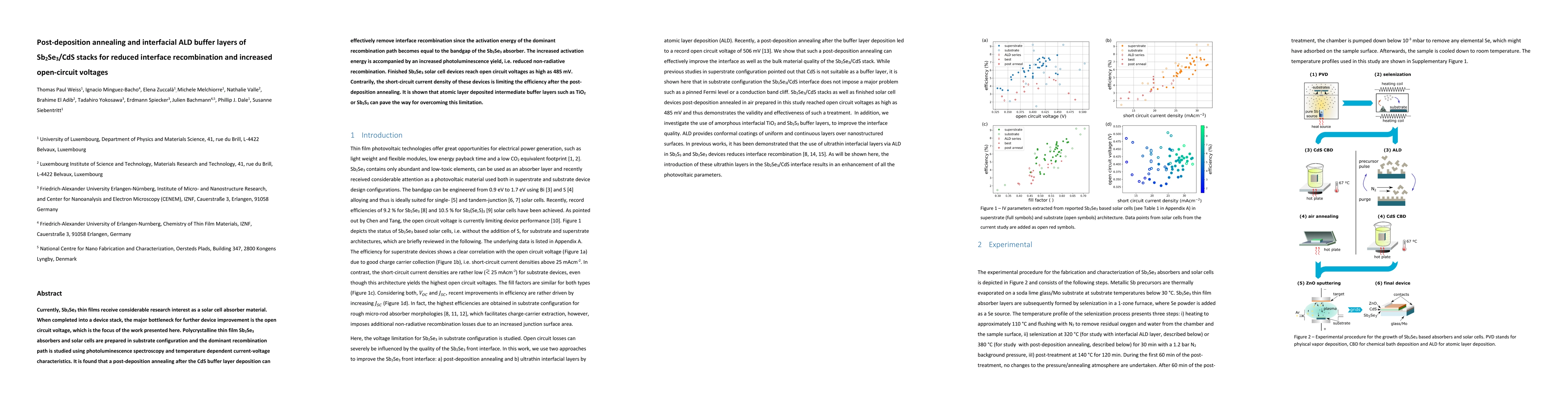
Currently, Sb$_2$Se$_3$ thin films receive considerable research interest as a solar cell absorber material. When completed into a device stack, the major bottleneck for further device improvement i...
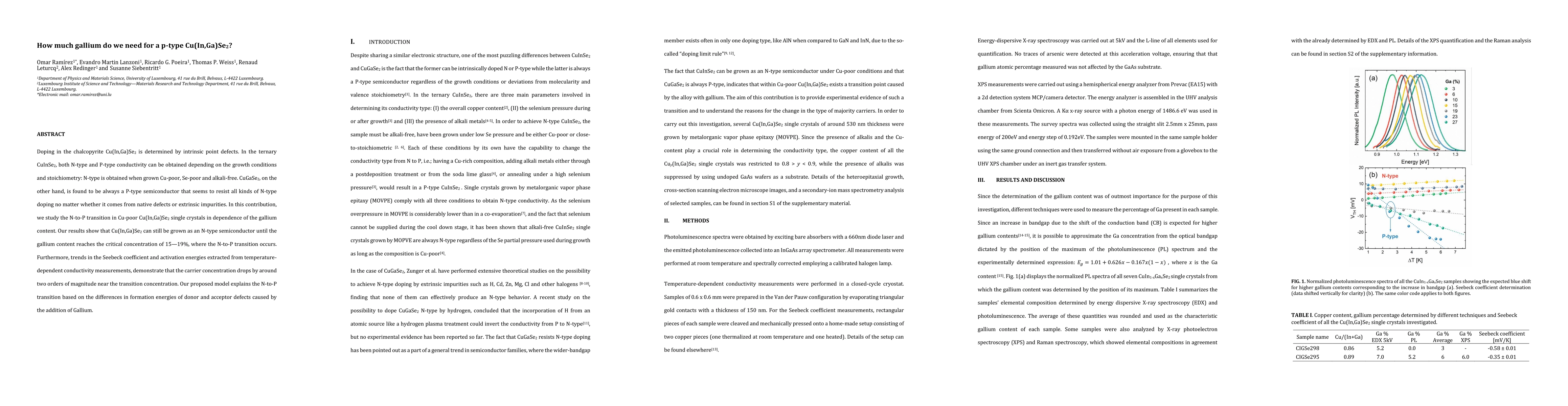
Doping in the chalcopyrite Cu(In,Ga)Se2 is determined by intrinsic point defects. In the ternary CuInSe2, both N-type and P-type conductivity can be obtained depending on the growth conditions and s...
Traditional CdS buffer layer in selenium-free Cu(In,Ga)S2 solar cells leads to reduced open-circuit voltage because of a negative conduction band offset at the Cu(In,Ga)S2/CdS interface. Reducing th...
Copper indium disulfide (CuInS$_2$) grown under Cu-rich conditions exhibits high optical quality but suffers predominantly from charge carrier interface recombination resulting in poor solar cell pe...
An in-depth understanding of the electronic properties of grain boundaries (GB) in polycrystalline semiconductor absorbers is of high importance since their charge carrier recombination rates may be...
The presence of interface recombination in a complex multilayered thin-film solar structure causes a disparity between the internal open-circuit voltage (VOC,in), measured by photoluminescence, and ...
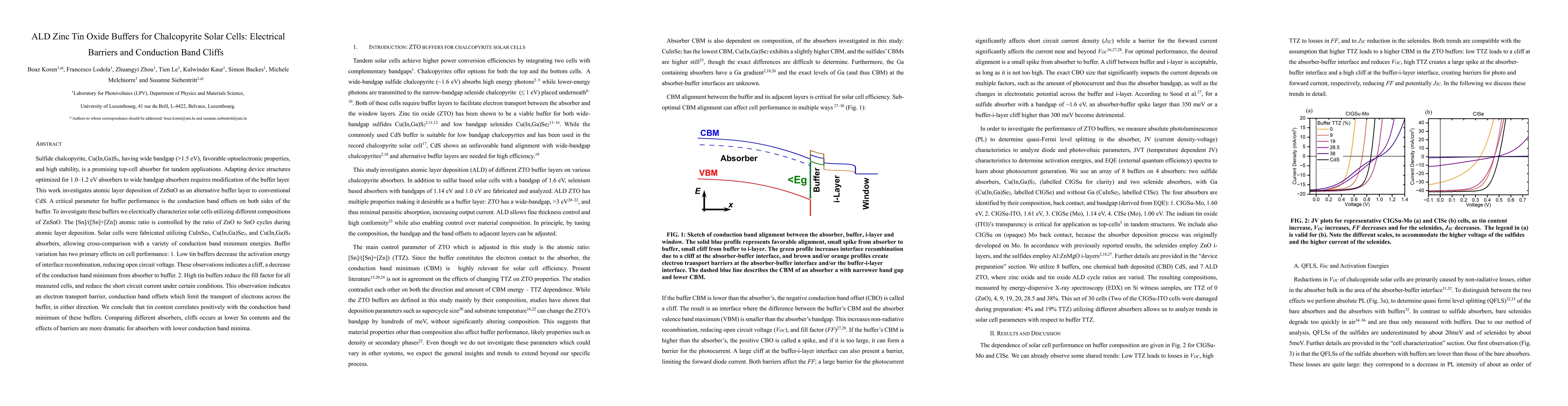
Interface recombination at the absorber buffer interface impedes the efficiency of a solar cell with an otherwise excellent absorber. The internal voltage or the quasi-Fermi level splitting (qFLs) m...
The radiative open circuit voltage loss in a solar cell occurs because the absorptance spectrum near the band gap shows gradual increase rather than sharp step function like transition. This broadenin...
Reducing the thickness of Cu(In,Ga)Se2 solar cells is a key objective in order to reduce production cost and to improve sustainability. The major challenge for sub-micron Cu(In,Ga)Se2 cells is the rec...
This study underscores the pivotal role of sodium (Na) supply in optimizing the optoelectronic properties of wide bandgap (~1.6 eV) Cu(In,Ga)S2 (CIGS) thin film absorbers for high efficiency solar cel...
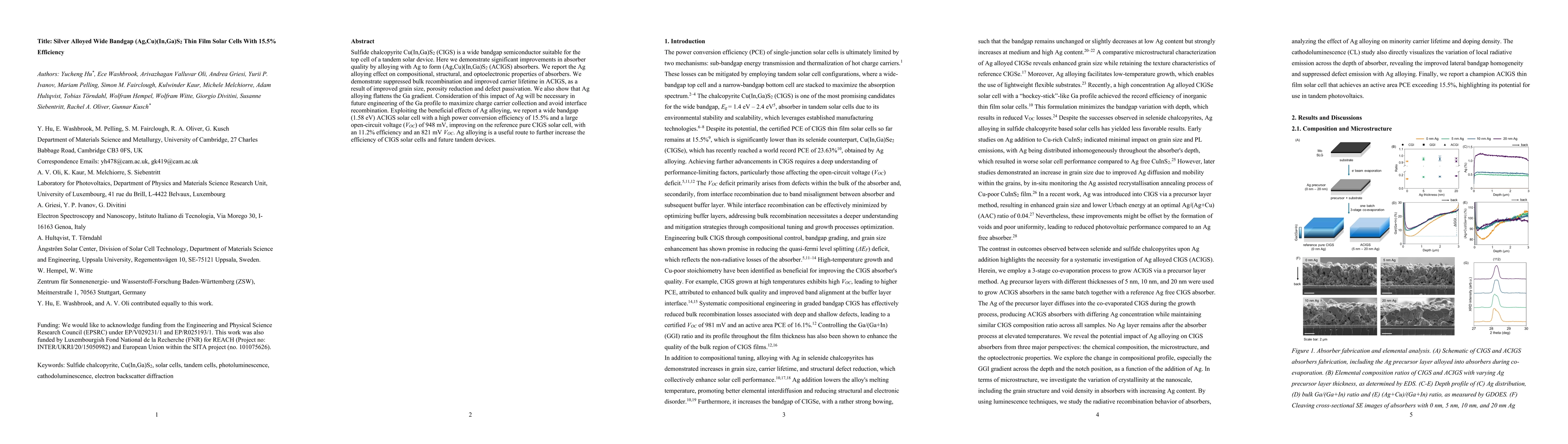
Sulfide chalcopyrite Cu(In,Ga)S2 (CIGS) is a wide bandgap semiconductor suitable for the top cell of a tandem solar device. Here we demonstrate significant improvements in absorber quality by alloying...
Sulfide chalcopyrite, Cu(In,Ga)S2, having wide bandgap (larger than 1.5 eV), favorable optoelectronic properties, and high stability, is a promising top-cell absorber for tandem applications. Adapting...
Tandem solar cells can better harness the energy of the solar spectrum. Chalcopyrite solar cells have drawn attention, being the only highly efficient devices with bandgap around 1.0 eV, suitable for ...
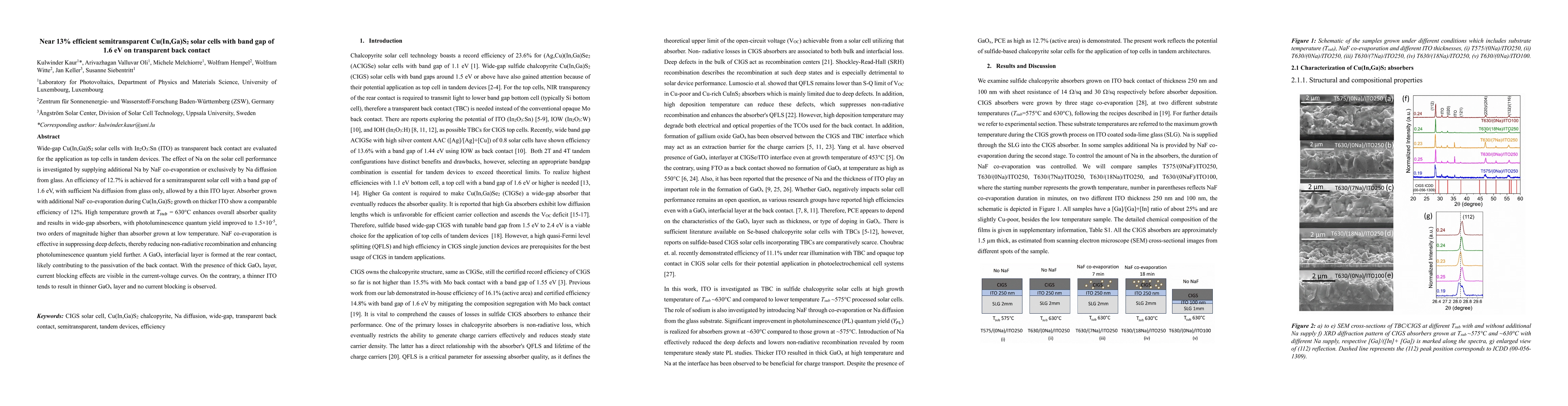
Wide-gap Cu(In,Ga)S2 solar cells with In2O3:Sn (ITO) as transparent back contact are evaluated for the application as top cells in tandem devices. The effect of Na on the solar cell performance is inv...
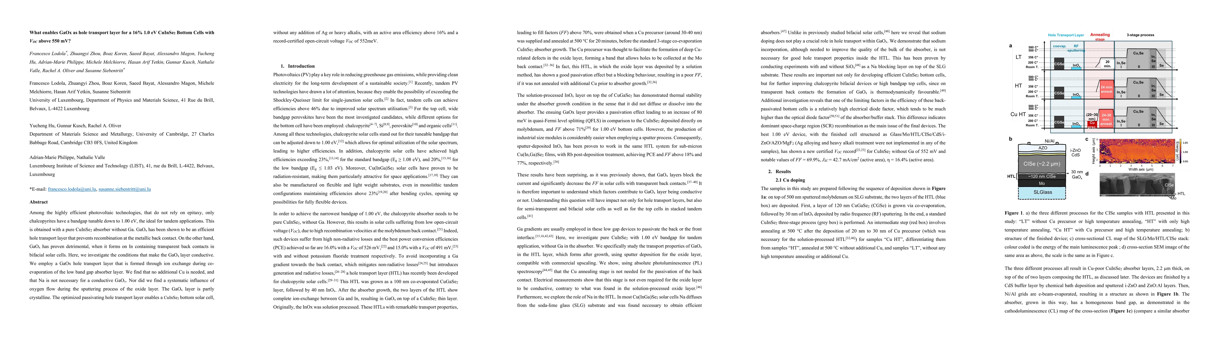
Among the highly efficient photovoltaic technologies, that do not rely on epitaxy, only chalcopyrites have a bandgap tunable down to 1.00 eV, the ideal for tandem applications. This is obtained with a...