ArxivLens
T
Researcher

Thilo Bauch

15 papers on arXiv

15 arXiv Papers
3 Total Publications
Profile

Academic Profile

Name T. Bauch
Total Papers 3
Scholar Profile View on Semantic Scholar
Metrics

Statistics

15 arXiv Papers
3 Total Publications
Publications

Papers on arXiv

Thumbnail for Current-phase relation of a short multi-mode Bi2Se3 topological
  insulator nanoribbon Josephson junction with ballistic transport modes
arXiv
Current-phase relation of a short multi-mode Bi2Se3 topological insulator nanoribbon Josephson junction with ballistic transport modes

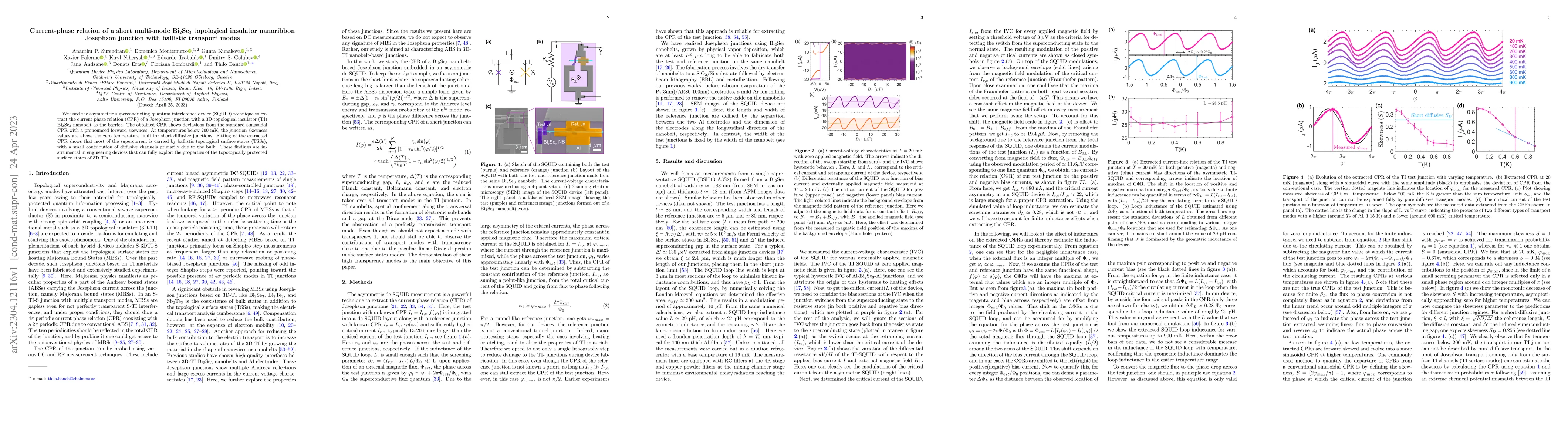
We used the asymmetric superconducting quantum interference device (SQUID) technique to extract the current phase relation (CPR) of a Josephson junction with a 3D-topological insulator (TI) Bi2Se3 n...

Thumbnail for Superconducting microsphere magnetically levitated in an anharmonic
  potential with integrated magnetic readout
arXiv
Superconducting microsphere magnetically levitated in an anharmonic potential with integrated magnetic readout

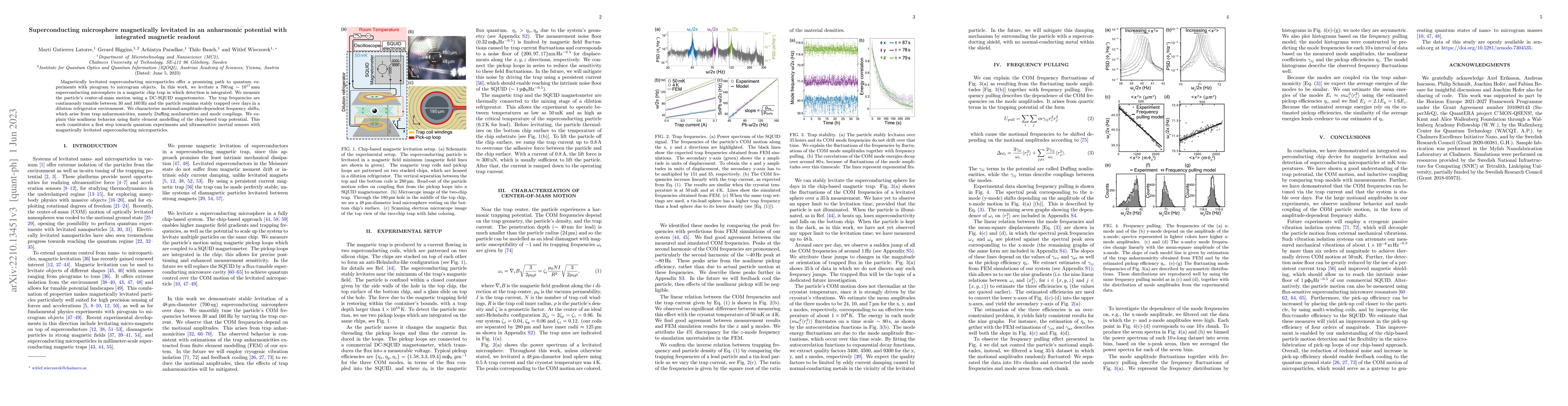
Magnetically levitated superconducting microparticles offer a promising path to quantum experiments with picogram to microgram objects. In this work, we levitate a 700ng $\sim 10^{17}$amu supercondu...

Thumbnail for Highly efficient UV detection in a metal-semiconductor-metal detector
  with epigraphene
arXiv
Highly efficient UV detection in a metal-semiconductor-metal detector with epigraphene

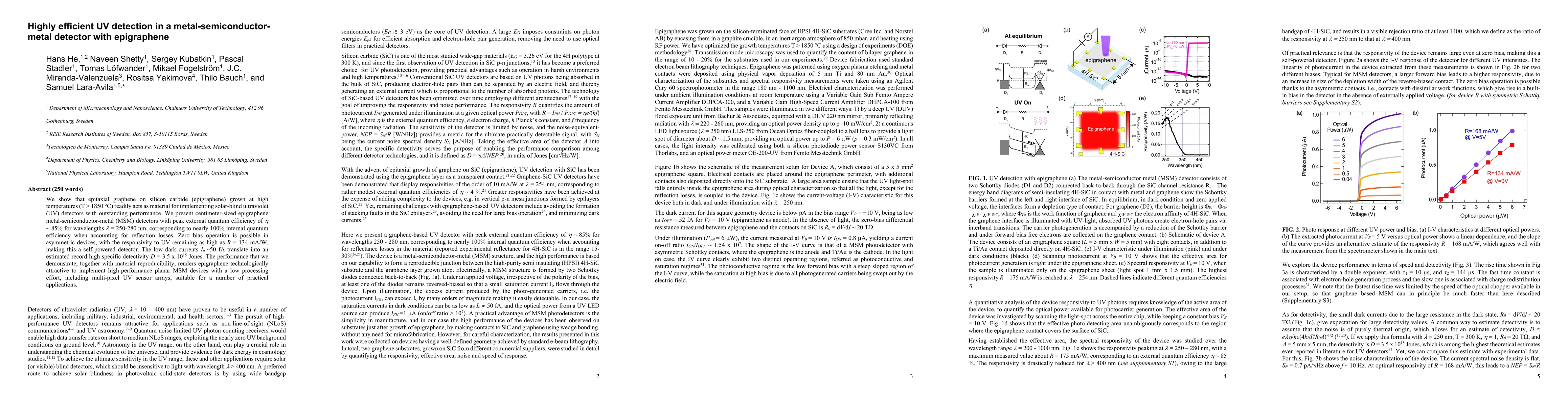
We show that epitaxial graphene on silicon carbide (epigraphene) grown at high temperatures (T > 1850 {\deg}C) readily acts as material for implementing solar-blind ultraviolet (UV) detectors with o...

Thumbnail for Gate-tunable hallmarks of unconventional superconductivity in
  non-centrosymmetric nanowires
arXiv
Gate-tunable hallmarks of unconventional superconductivity in non-centrosymmetric nanowires

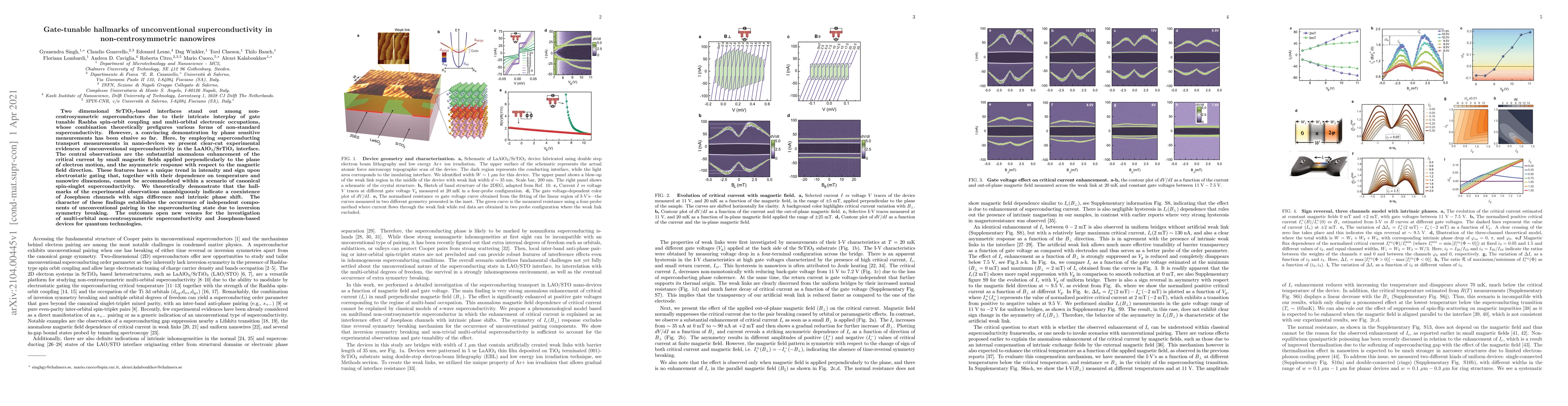
Two dimensional SrTiO3-based interfaces stand out among non-centrosymmetric superconductors due to their intricate interplay of gate tunable Rashba spin-orbit coupling and multi-orbital electronic o...

Thumbnail for Stoichiometric Bi2Se3 Topological Insulator Ultra-Thin Films Obtained
  Through a New Fabrication Process for Optoelectronic Applications
arXiv
Stoichiometric Bi2Se3 Topological Insulator Ultra-Thin Films Obtained Through a New Fabrication Process for Optoelectronic Applications

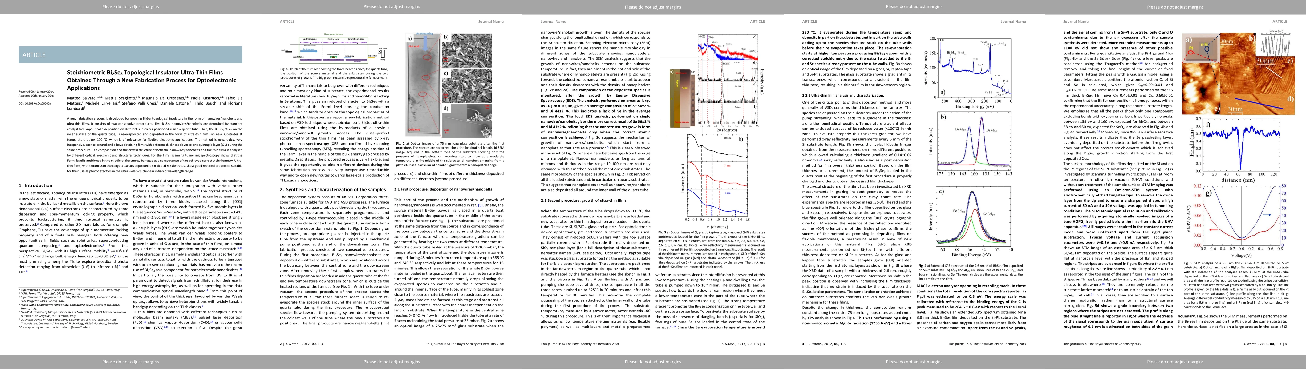
A new fabrication process is developed for growing Bi2Se3 topological insulators in the form of nanowires/nanobelts and ultra-thin films. It consists of two consecutive procedures: first Bi2Se3 nano...

Thumbnail for Tailoring Superconductivity in Large-Area Single-Layer NbSe2 via
  Self-Assembled Molecular Adlayers
arXiv
Tailoring Superconductivity in Large-Area Single-Layer NbSe2 via Self-Assembled Molecular Adlayers

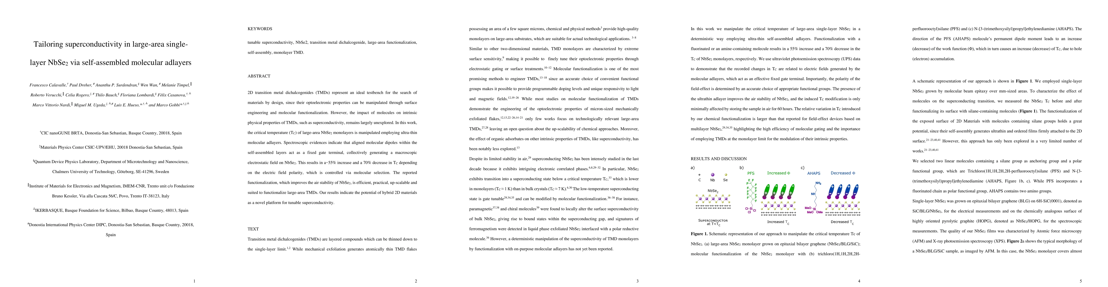
Two-dimensional transition metal dichalcogenides (TMDs) represent an ideal testbench for the search of materials by design, because their optoelectronic properties can be manipulated through surface...

Thumbnail for Topological insulator nanoribbon Josephson junctions: evidence for size
  effect in transport properties
arXiv
Topological insulator nanoribbon Josephson junctions: evidence for size effect in transport properties

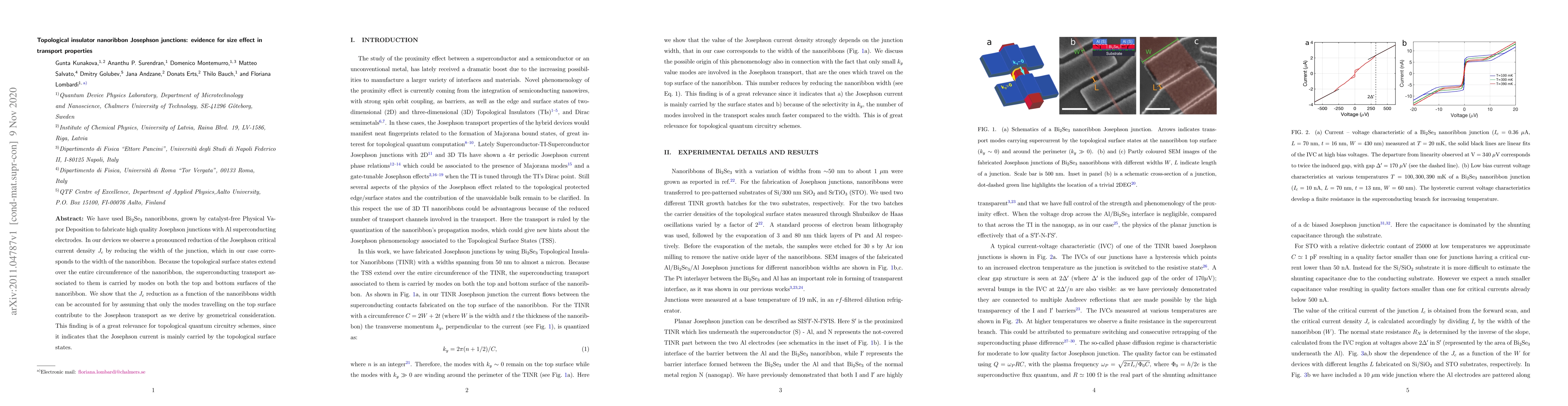
We have used Bi$_2$Se$_3$ nanoribbons, grown by catalyst-free Physical Vapor Deposition to fabricate high quality Josephson junctions with Al superconducting electrodes. In our devices we observe a ...

Thumbnail for The performance limits of epigraphene Hall sensors
arXiv
The performance limits of epigraphene Hall sensors

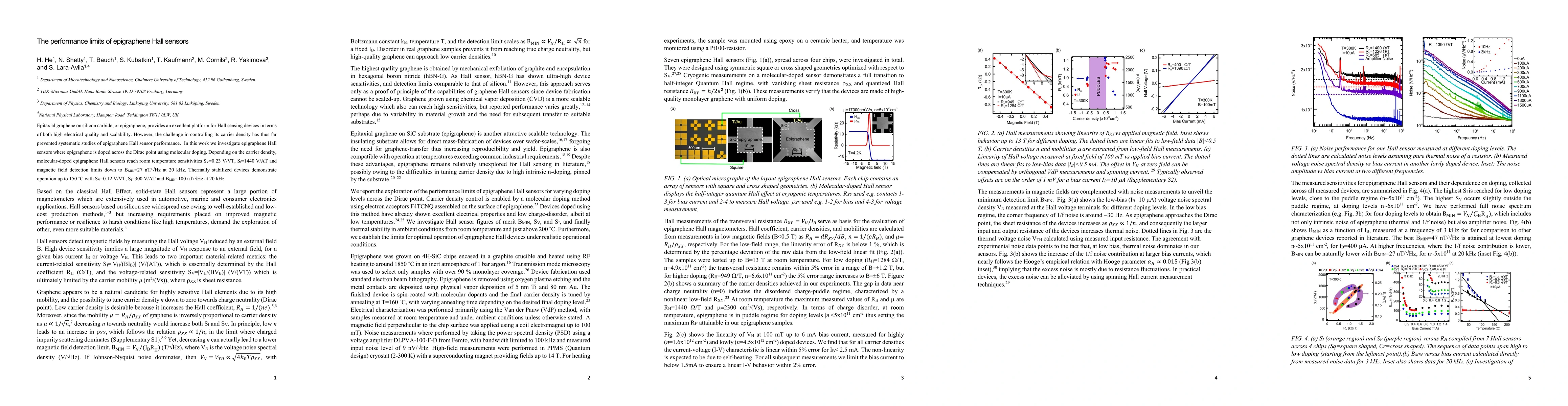
Epitaxial graphene on silicon carbide, or epigraphene, provides an excellent platform for Hall sensing devices in terms of both high electrical quality and scalability. However, the challenge in con...

Thumbnail for Fabrication and electrical transport characterization of high quality
  underdoped YBa$_2$Cu$_3$O$_{7-{\delta}}$ nanowires
arXiv
Fabrication and electrical transport characterization of high quality underdoped YBa$_2$Cu$_3$O$_{7-{\delta}}$ nanowires

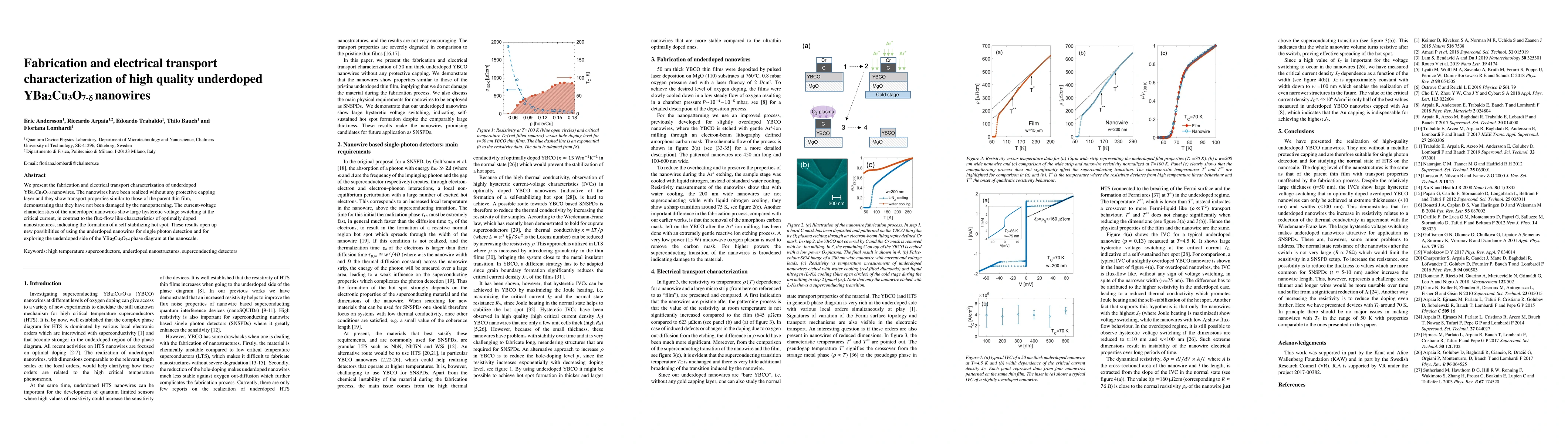
We present the fabrication and electrical transport characterization of underdoped YBa$_2$Cu$_3$O$_{7-{\delta}}$ nanowires. The nanowires have been realized without any protective capping layer and ...

Thumbnail for SQUID magnetometer based on Grooved Dayem nanobridges and a flux
  transformer
arXiv
SQUID magnetometer based on Grooved Dayem nanobridges and a flux transformer

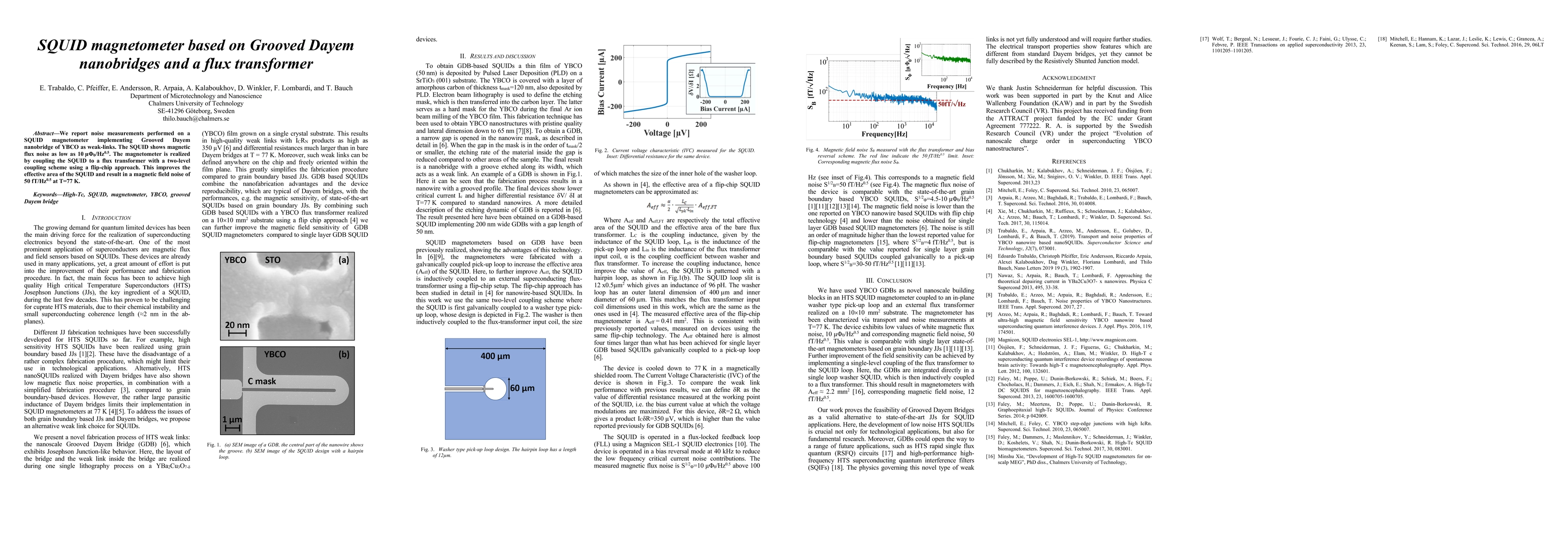
We report noise measurements performed on a SQUID magnetometer implementing Grooved Dayem nanobridge of YBCO as weak-links. The SQUID shows magnetic flux noise as low as 10 $\mu \Phi_0$/Hz$^{0.5}$. ...

Thumbnail for On the Angular Dependence of InP High Electron Mobility Transistors for
  Cryogenic Low Noise Amplifiers in a Magnetic Field
arXiv
On the Angular Dependence of InP High Electron Mobility Transistors for Cryogenic Low Noise Amplifiers in a Magnetic Field

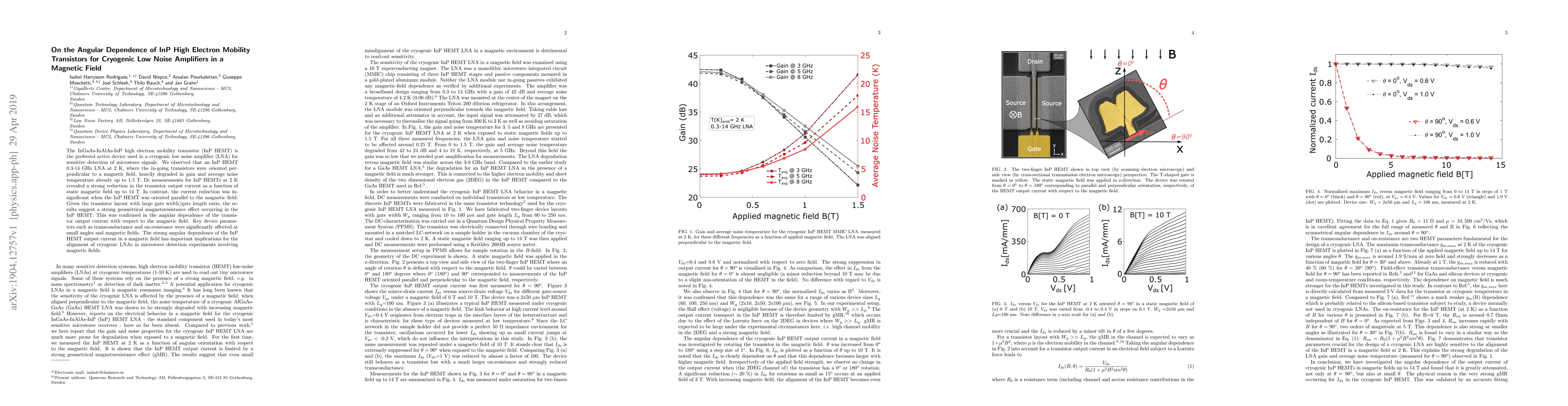
The InGaAs-InAlAs-InP high electron mobility transistor (InP HEMT) is the preferred active device used in a cryogenic low noise amplifier (LNA) for sensitive detection of microwave signals. We obser...

Thumbnail for Grooved Dayem nanobridges as building blocks of high-performance
  YBa$_2$Cu$_3$O$_{7-\delta}$ SQUID magnetometers
arXiv
Grooved Dayem nanobridges as building blocks of high-performance YBa$_2$Cu$_3$O$_{7-\delta}$ SQUID magnetometers

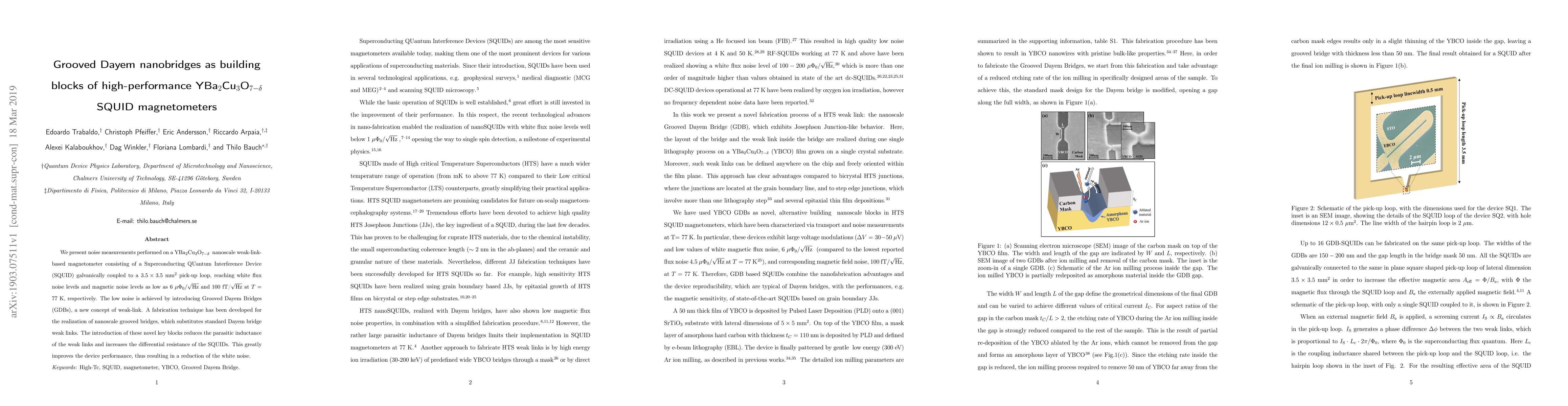
We present noise measurements performed on a YBa$_2$Cu$_3$O$_{7-\delta}$ nanoscale weak-link-based magnetometer consisting of a Superconducting QUantum Interference Device (SQUID) galvanically coupl...

Thumbnail for Boosting superconductivity: how nanofaceted surfaces transform the
  ground state of ultrathin YBa$_2$Cu$_3$O$_{7-δ}$ thin films
arXiv
Boosting superconductivity: how nanofaceted surfaces transform the ground state of ultrathin YBa$_2$Cu$_3$O$_{7-δ}$ thin films

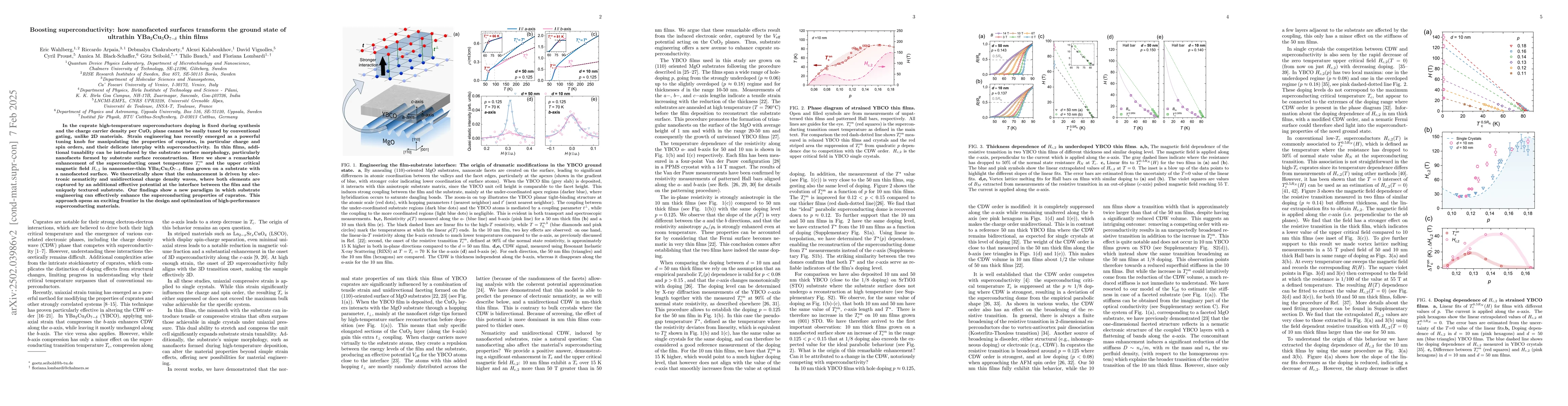
In the cuprate high-temperature superconductors doping is fixed during synthesis and the charge carrier density per CuO$_2$ plane cannot be easily tuned by conventional gating, unlike 2D materials. St...

Thumbnail for THz mixing of high-order harmonics using $YBa_2Cu_3O_{7-δ}$
  nanobridges
arXiv
THz mixing of high-order harmonics using $YBa_2Cu_3O_{7-δ}$ nanobridges

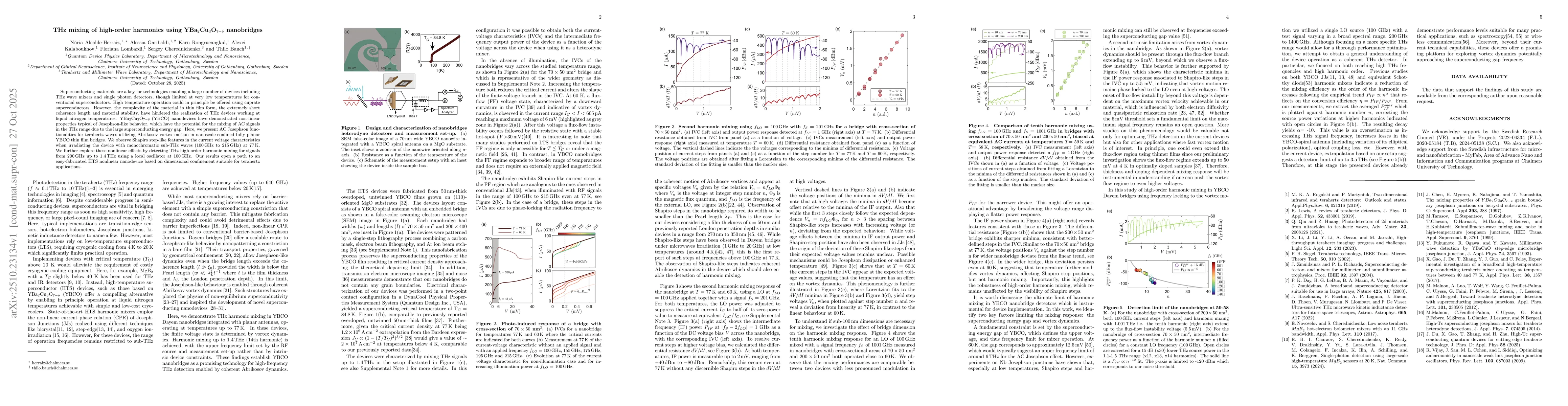
Superconducting materials are a key for technologies enabling a large number of devices including THz wave mixers and single photon detectors, though limited at very low temperatures for conventional ...

Thumbnail for Wafer-Scale Single-Crystalline Monolayer Graphene
arXiv
Wafer-Scale Single-Crystalline Monolayer Graphene

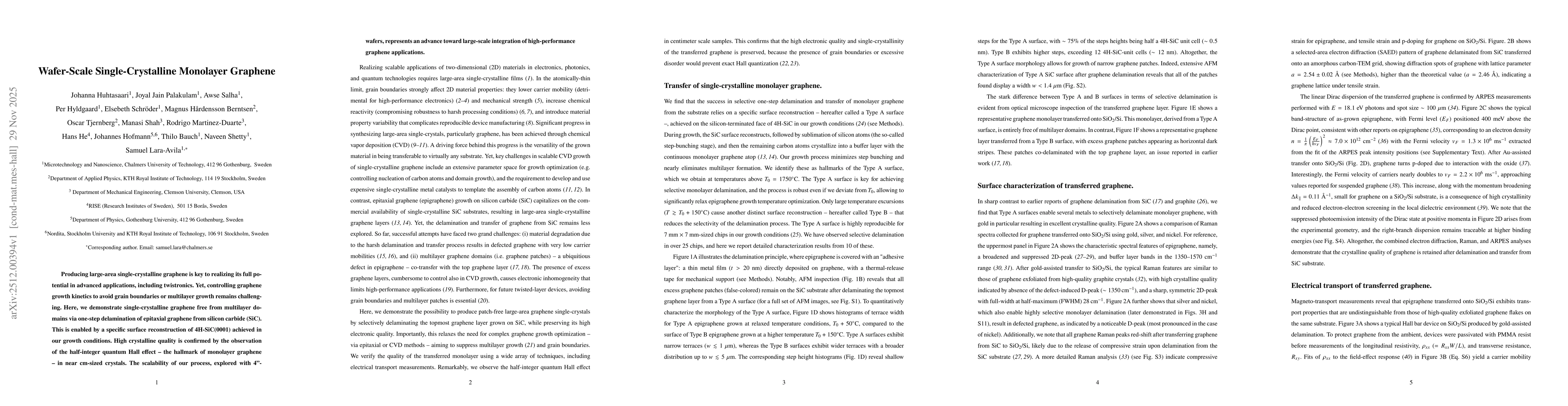
Producing large-area single-crystalline graphene is key to realizing its full potential in advanced applications, including twistronics. Yet, controlling graphene growth kinetics to avoid grain bounda...
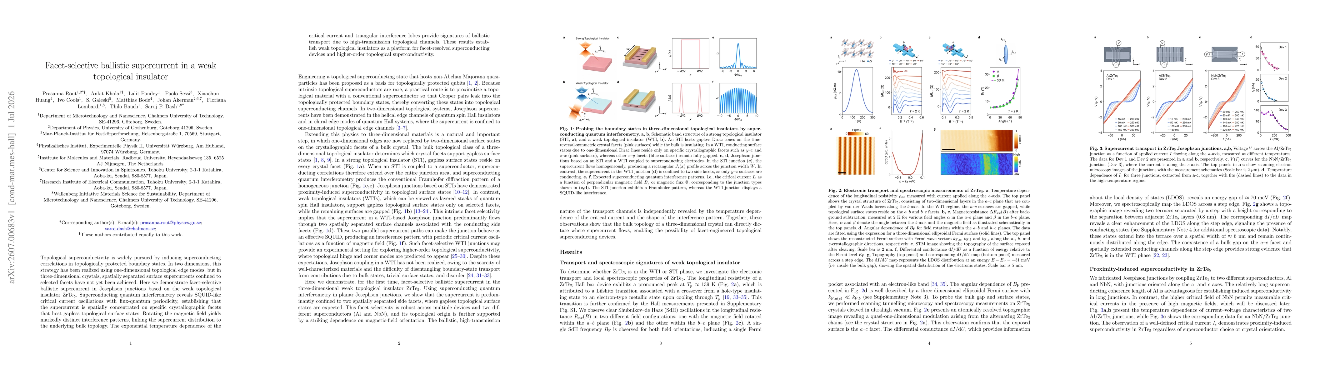
This website uses cookies to ensure you get the best experience. Learn more