Academic Profile
Statistics
Similar Authors
Papers on arXiv
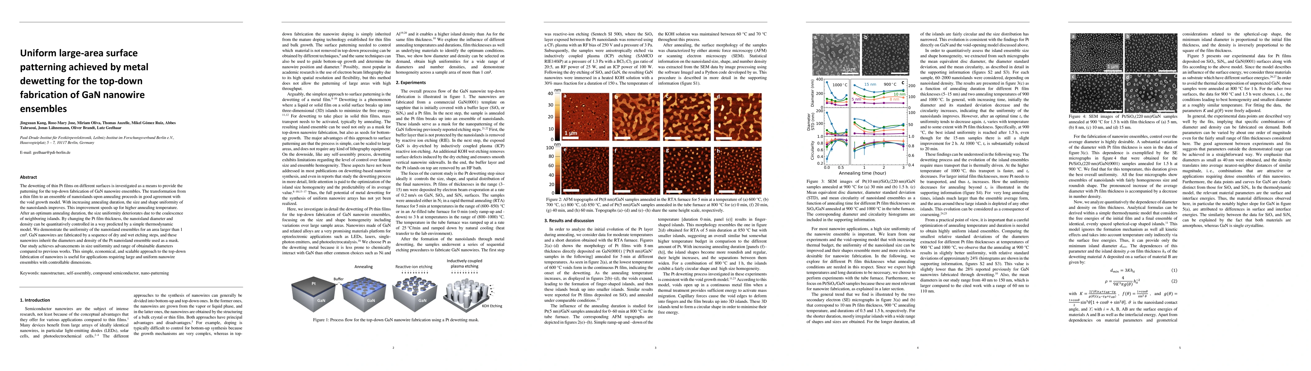
The dewetting of thin Pt films on different surfaces is investigated as a means to provide the patterning for the top-down fabrication of GaN nanowire ensembles. The transformation from a thin film ...
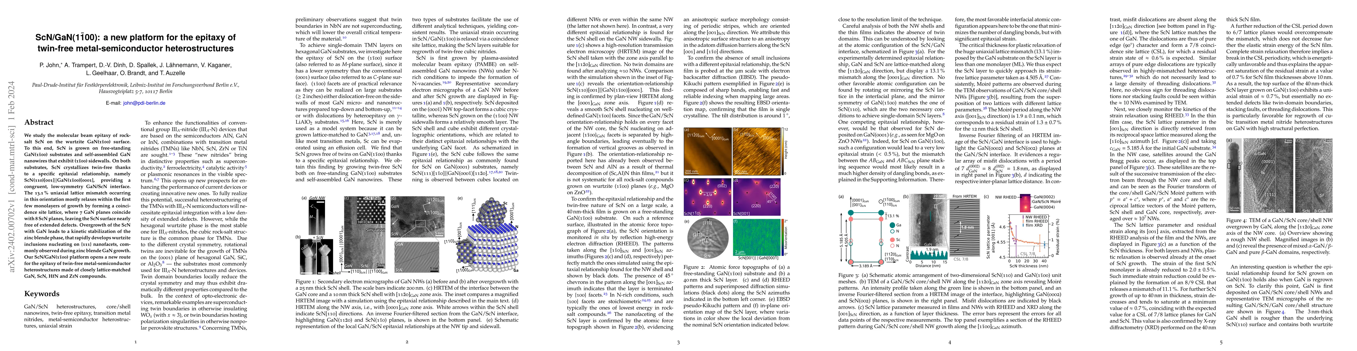
We study the molecular beam epitaxy of rock-salt ScN on the wurtzite GaN($1\bar{1}00$) surface. To this end, ScN is grown on free-standing GaN($1\bar{1}00$) substrates and self-assembled GaN nanowir...
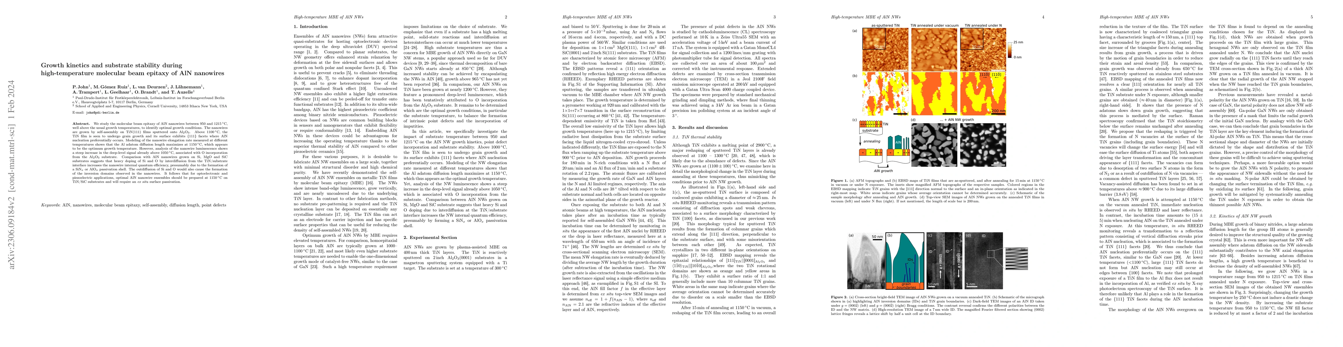
We study the molecular beam epitaxy of AlN nanowires between 950 and 1215 {\deg}C, well above the usual growth temperatures, to identify optimal growth conditions. The nanowires are grown by self-as...
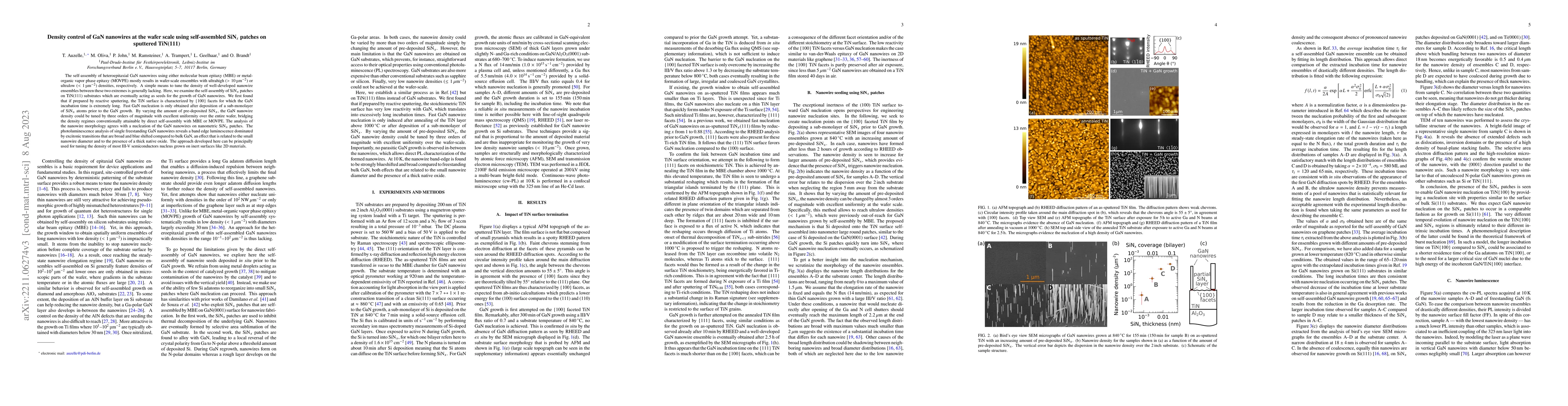
The self-assembly of heteroepitaxial GaN nanowires using either molecular beam epitaxy (MBE) or metal-organic vapor phase epitaxy (MOVPE) mostly results in wafer-scale ensembles with ultrahigh ($>10...
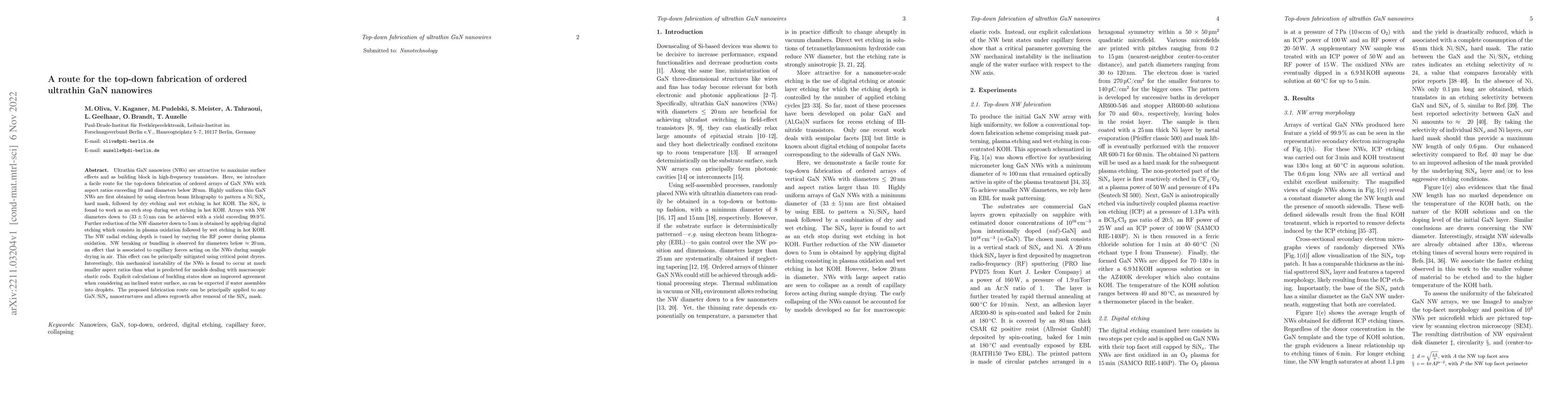
Ultrathin GaN nanowires (NWs) are attractive to maximize surface effects and as building block in high-frequency transistors. Here, we introduce a facile route for the top-down fabrication of ordere...
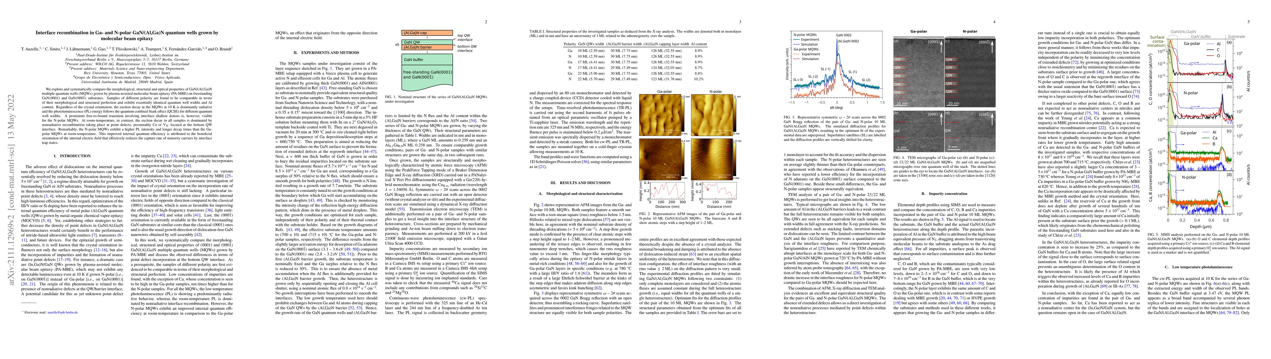
We explore and systematically compare the morphological, structural and optical properties of GaN/(Al,Ga)N multiple quantum wells (MQWs) grown by plasma-assisted molecular beam epitaxy (PA-MBE) on f...
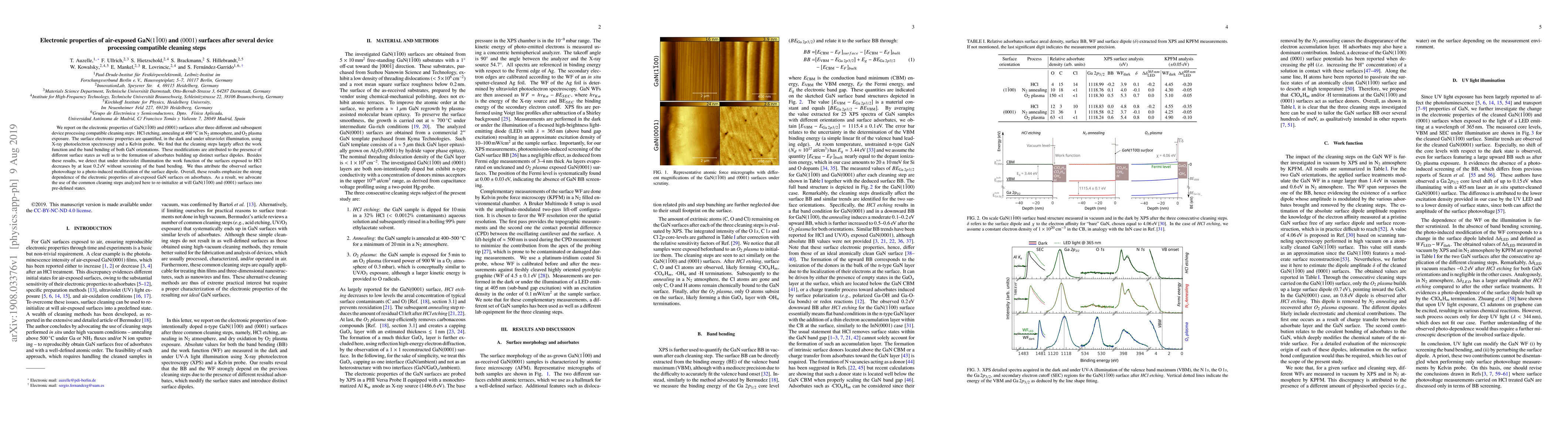
We report on the electronic properties of GaN$(1\bar{1}00)$ and $(0001)$ surfaces after three different and subsequent device processing compatible cleaning steps: HCl etching, annealing at $400$ $^...
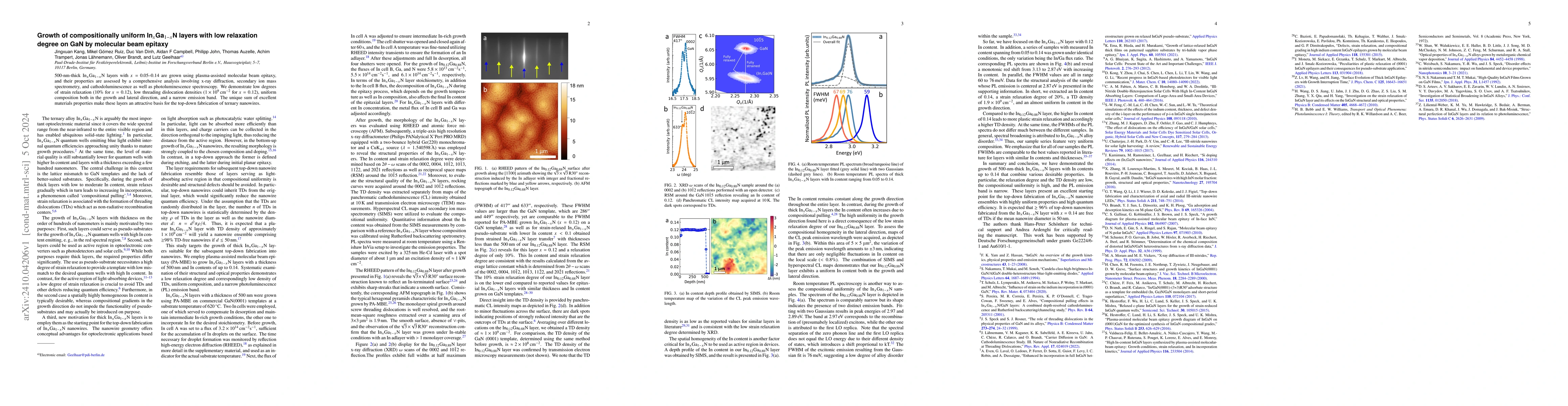
500-nm-thick $\mathrm{In}_{x}\mathrm{Ga}_{1-x}\mathrm{N}$ layers with $x=$ 0.05-0.14 are grown using plasma-assisted molecular beam epitaxy, and their properties are assessed by a comprehensive analys...
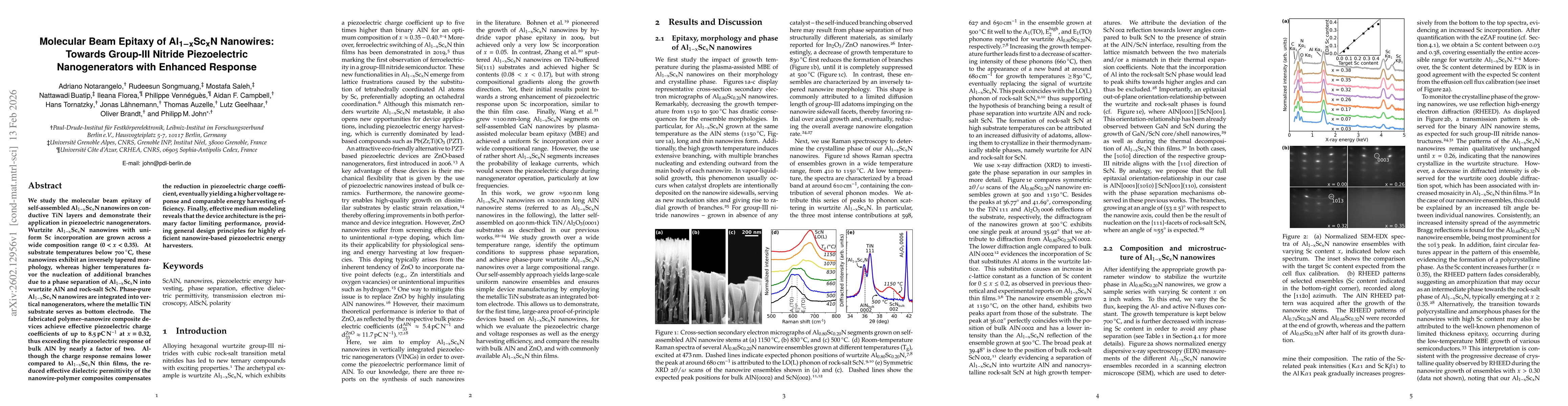
We study the molecular beam epitaxy of self-assembled Al$\mathrm{_{1-x}}$Sc$\mathrm{_{x}}$N nanowires on conductive TiN layers and demonstrate their application in piezoelectric nanogenerators. Wurtzi...