ArxivLens
T
Researcher

Thomas E. Beechem

10 papers on arXiv

10 arXiv Papers
192 Total Publications
Profile

Academic Profile

Name T. Beechem
Total Papers 192
Scholar Profile View on Semantic Scholar
Metrics

Statistics

10 arXiv Papers
192 Total Publications
Publications

Papers on arXiv

Thumbnail for Material Characteristics Governing In-Plane Phonon-Polariton Thermal
  Conductance
arXiv
Material Characteristics Governing In-Plane Phonon-Polariton Thermal Conductance

The material dependence of phonon-polariton based in-plane thermal conductance is investigated by examining systems composed of air and several wurtzite and zinc-blende crystals. Phonon-polariton ba...

Thumbnail for Near-field Imaging of Optical Resonances in Silicon Metasurfaces Using
  Photoelectron Microscopy
arXiv
Near-field Imaging of Optical Resonances in Silicon Metasurfaces Using Photoelectron Microscopy

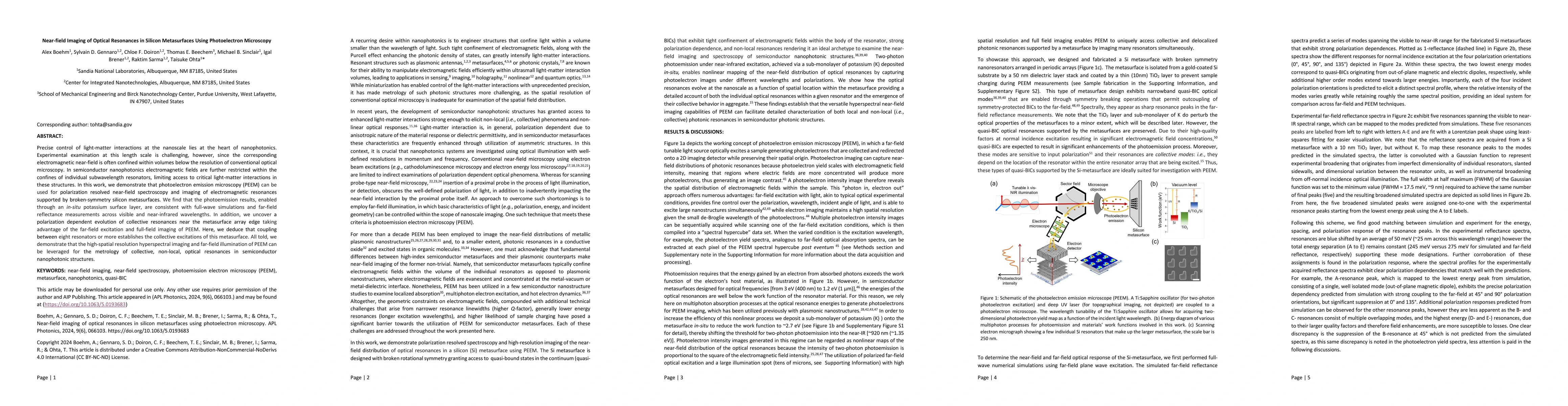
Precise control of light-matter interactions at the nanoscale lies at the heart of nanophotonics. Experimental examination at this length scale is challenging, however, since the corresponding elect...

Thumbnail for Growth of Ultrathin Bi$_2$Se$_3$ Films by Molecular Beam Epitaxy
arXiv
Growth of Ultrathin Bi$_2$Se$_3$ Films by Molecular Beam Epitaxy

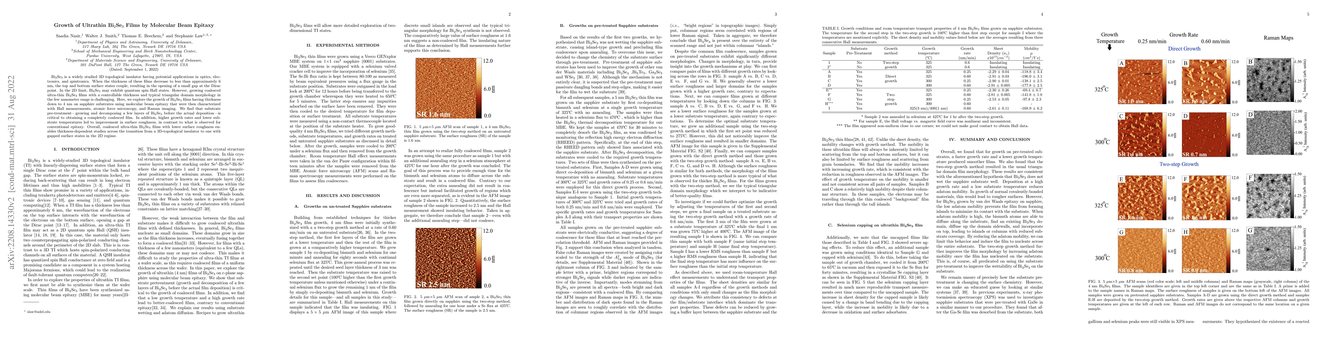
Bi$_2$Se$_3$ is a widely studied 3D topological insulator having potential applications in optics, electronics, and spintronics. When the thickness of these films decrease to less than approximately...

Thumbnail for Detection of High Energy Ionizing Radiation using Deeply Depleted
  Graphene-Oxide-Semiconductor Junctions
arXiv
Detection of High Energy Ionizing Radiation using Deeply Depleted Graphene-Oxide-Semiconductor Junctions

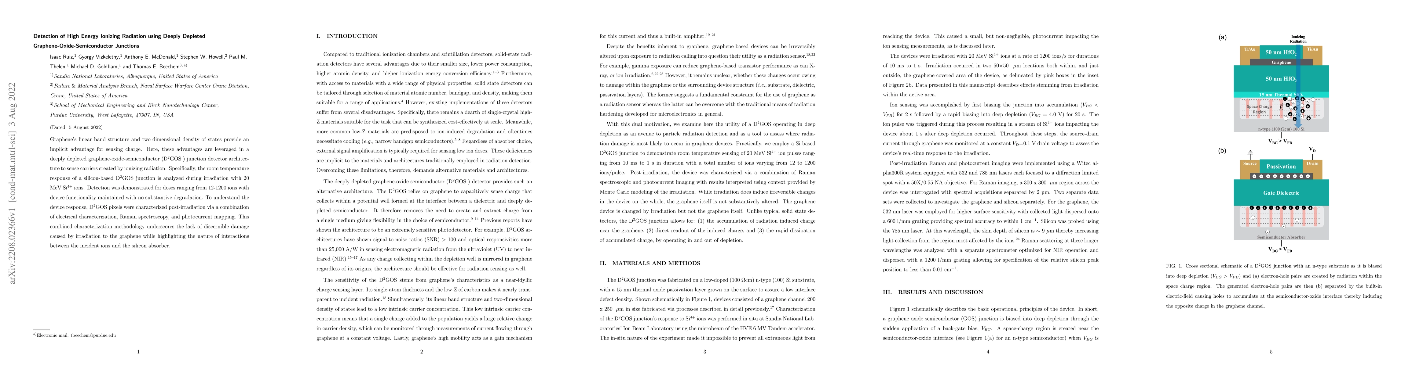
Graphene's linear bandstructure and two-dimensional density of states provide an implicit advantage for sensing charge. Here, these advantages are leveraged in a deeply depleted graphene-oxide-semic...

Thumbnail for Nanoscale Phonon Spectroscopy Reveals Emergent Interface Vibrational
  Structure of Superlattices
arXiv
Nanoscale Phonon Spectroscopy Reveals Emergent Interface Vibrational Structure of Superlattices

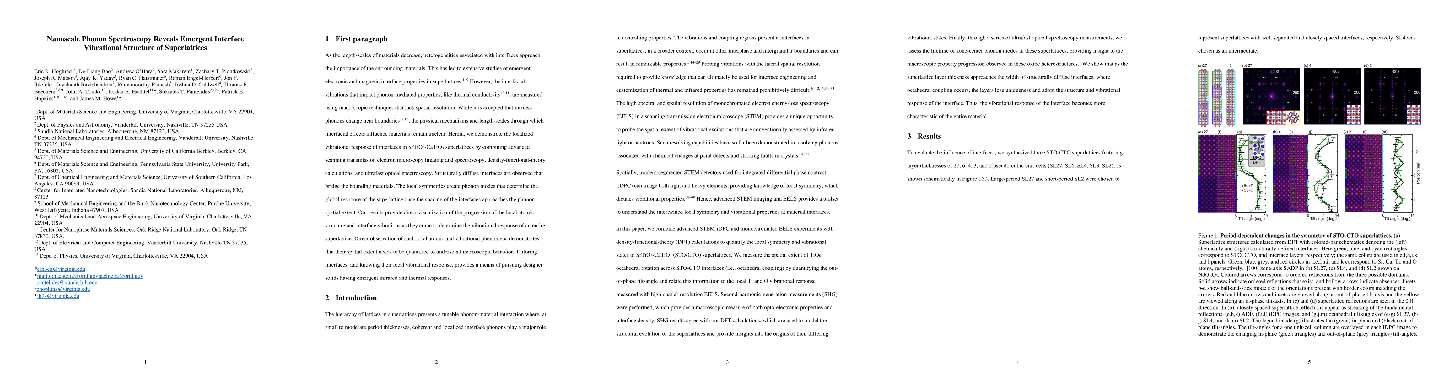
As the length-scales of materials decrease, heterogeneities associated with interfaces approach the importance of the surrounding materials. Emergent electronic and magnetic interface properties in ...

Thumbnail for Photo-physics and electronic structure of lateral graphene/MoS2 and
  metal/MoS2 junctions
arXiv
Photo-physics and electronic structure of lateral graphene/MoS2 and metal/MoS2 junctions

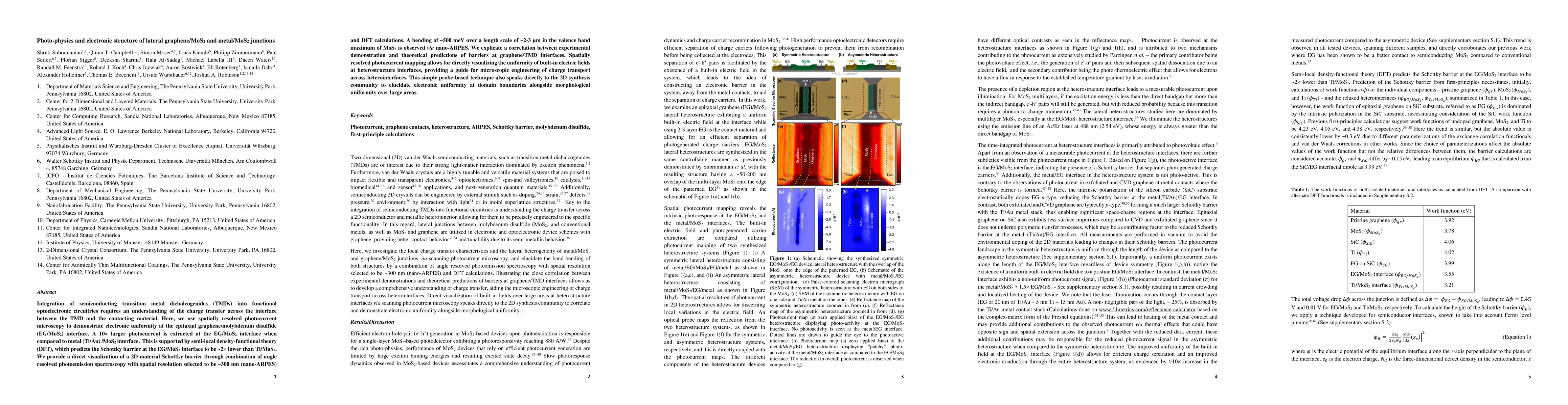
Integration of semiconducting transition metal dichalcogenides (TMDs) into functional optoelectronic circuitries requires an understanding of the charge transfer across the interface between the TMD...

Thumbnail for Nitrogen Vacancies Induce Fatigue in Ferroelectric
  $\mathrm{Al_{0.93}B_{0.07}N}$
arXiv
Nitrogen Vacancies Induce Fatigue in Ferroelectric $\mathrm{Al_{0.93}B_{0.07}N}$

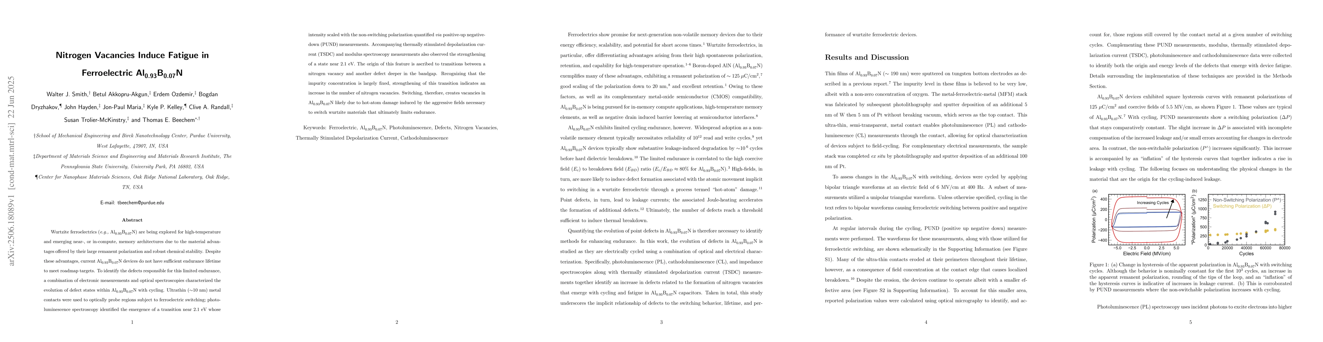
Wurtzite ferroelectrics (e.g., $\mathrm{Al_{0.93}B_{0.07}N}$) are being explored for high-temperature and emerging near-, or in-compute, memory architectures due to the material advantages offered by ...

Thumbnail for Tuning Breakdown-to-Coercive Field Ratio in Ultra-Thin Al1-xScxN Films via Reactive Nitrogen Atmosphere
arXiv
Tuning Breakdown-to-Coercive Field Ratio in Ultra-Thin Al1-xScxN Films via Reactive Nitrogen Atmosphere

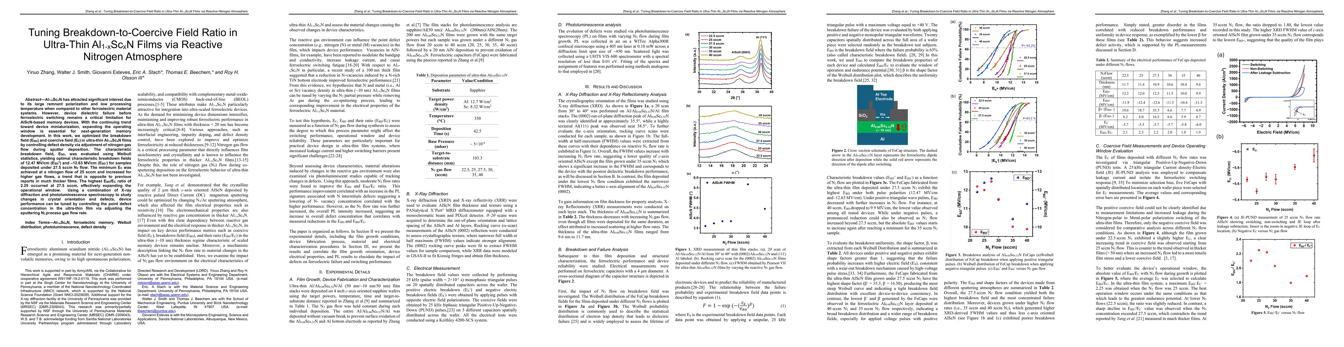
Al1-xScxN has attracted significant interest due to its large remnant polarization and low processing temperature when compared to other ferroelectric material systems. However, device dielectric fail...

Thumbnail for Cross-hatch strain effects on SiGe quantum dots for qubit variability estimation
arXiv
Cross-hatch strain effects on SiGe quantum dots for qubit variability estimation

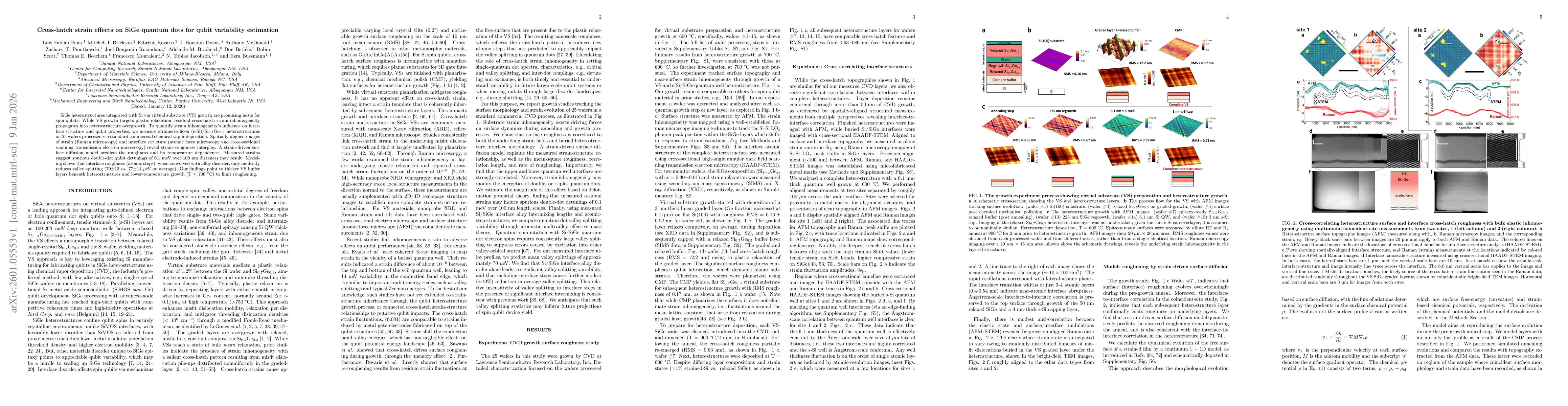
SiGe heterostructures integrated with Si via virtual substrate (VS) growth are promising hosts for spin qubits. While VS growth targets plastic relaxation, residual cross-hatch strain inhomogeneity pr...

Thumbnail for Seed Layer Engineering for Effective Charge Transfer Doping of MoS$_2$ Transistors
arXiv
Seed Layer Engineering for Effective Charge Transfer Doping of MoS$_2$ Transistors

Integrating two-dimensional semiconductors such as MoS$_2$ with dielectric materials remains a central challenge for their use in future logic technologies. While seed layers are typically introduced ...

This website uses cookies to ensure you get the best experience. Learn more