Academic Profile
Statistics
Similar Authors
Papers on arXiv
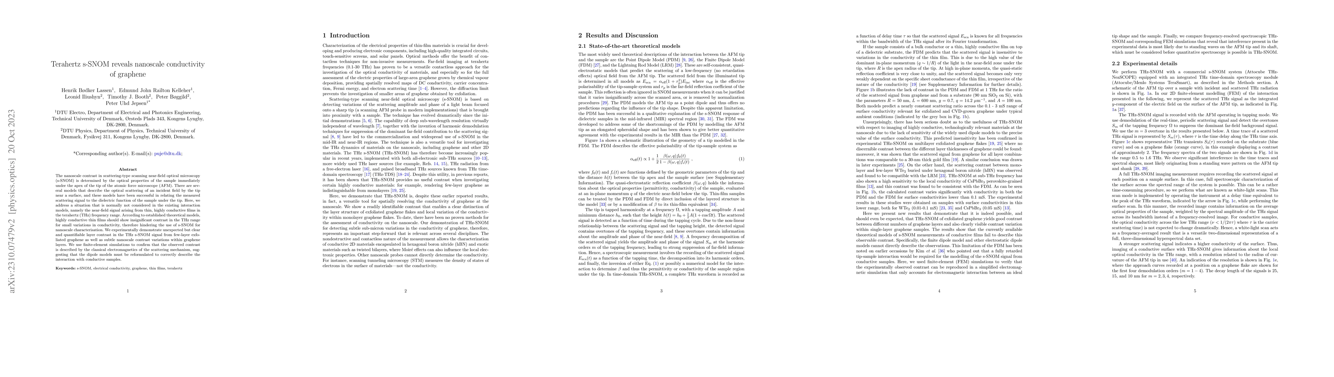
The nanoscale contrast in scattering-type scanning near-field optical microscopy (s-SNOM) is determined by the optical properties of the sample immediately under the apex of the tip of the atomic fo...
Strong Fermi level pinning (FLP) - often attributed to metal-induced gap states at the interfacial contacts - severely reduces the tunability of the Schottky barrier height of the junction and limit...
Cathodoluminescence spectroscopy in conjunction with second-order auto-correlation measurements of $g_2(\tau)$ allows to extensively study the synchronization of quantum light sources in low-dimensi...
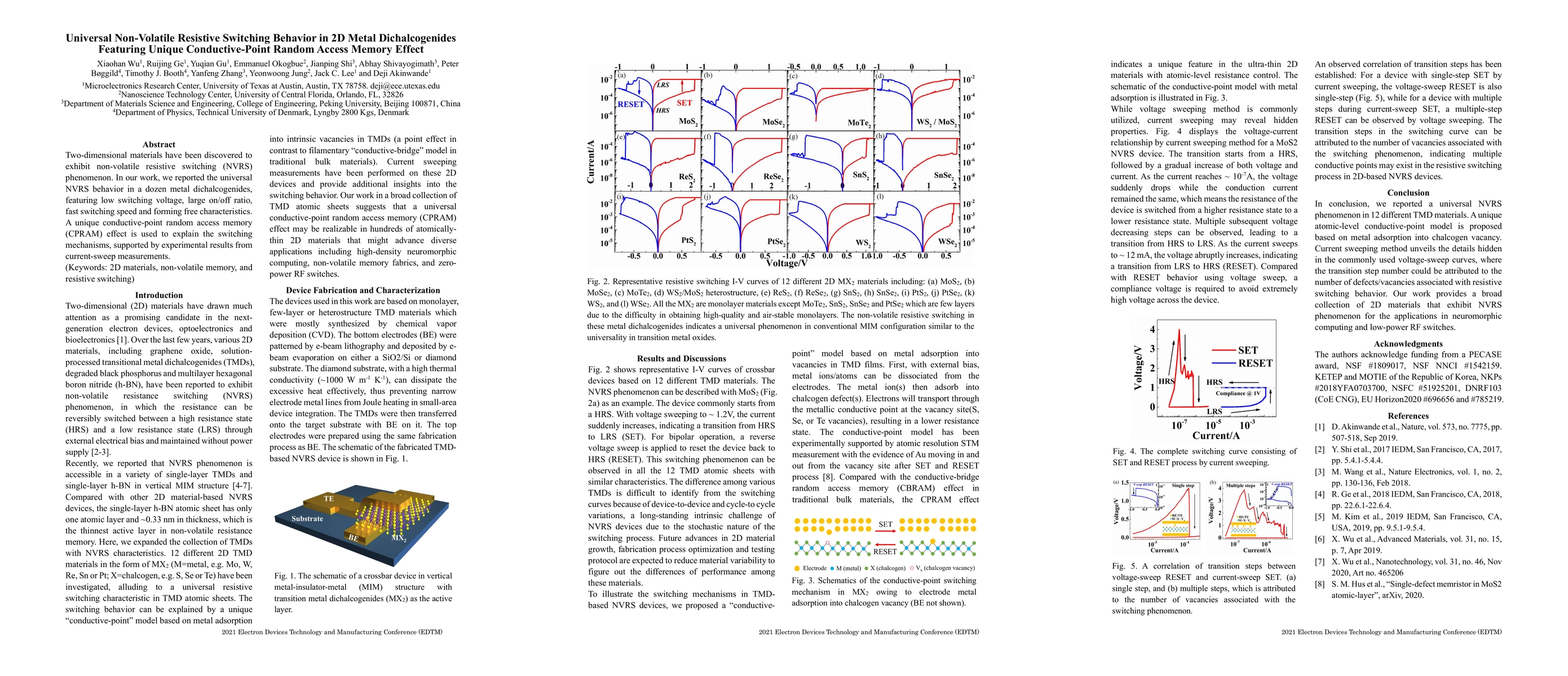
Two-dimensional materials have been discovered to exhibit non-volatile resistive switching (NVRS) phenomenon. In our work, we reported the universal NVRS behavior in a dozen metal dichalcogenides, f...
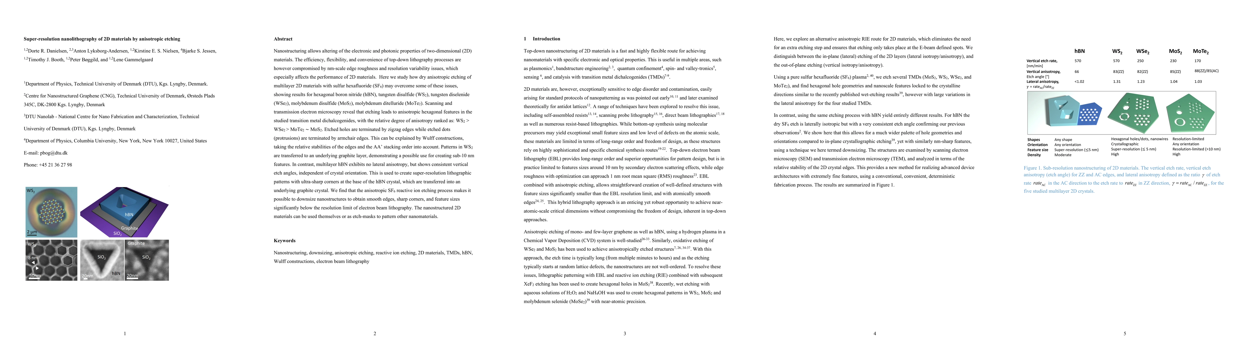
Nanostructuring allows altering of the electronic and photonic properties of two-dimensional (2D) materials. The efficiency, flexibility, and convenience of top-down lithography processes are howeve...
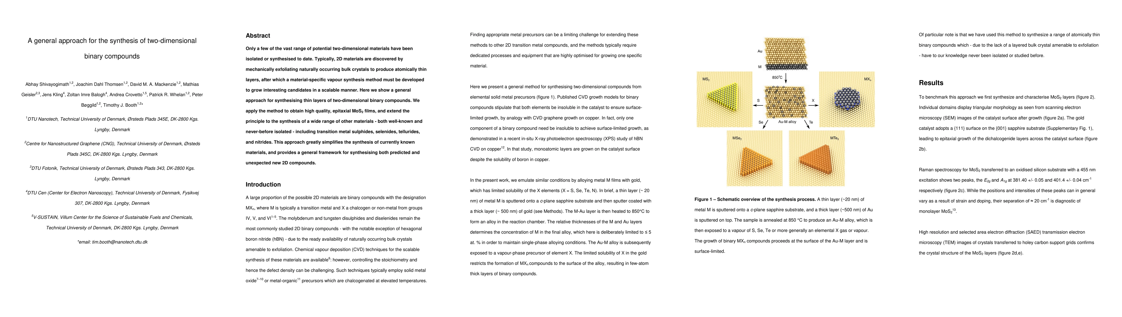
Only a few of the vast range of potential two-dimensional materials have been isolated or synthesised to date. Typically, 2D materials are discovered by mechanically exfoliating naturally occurring ...
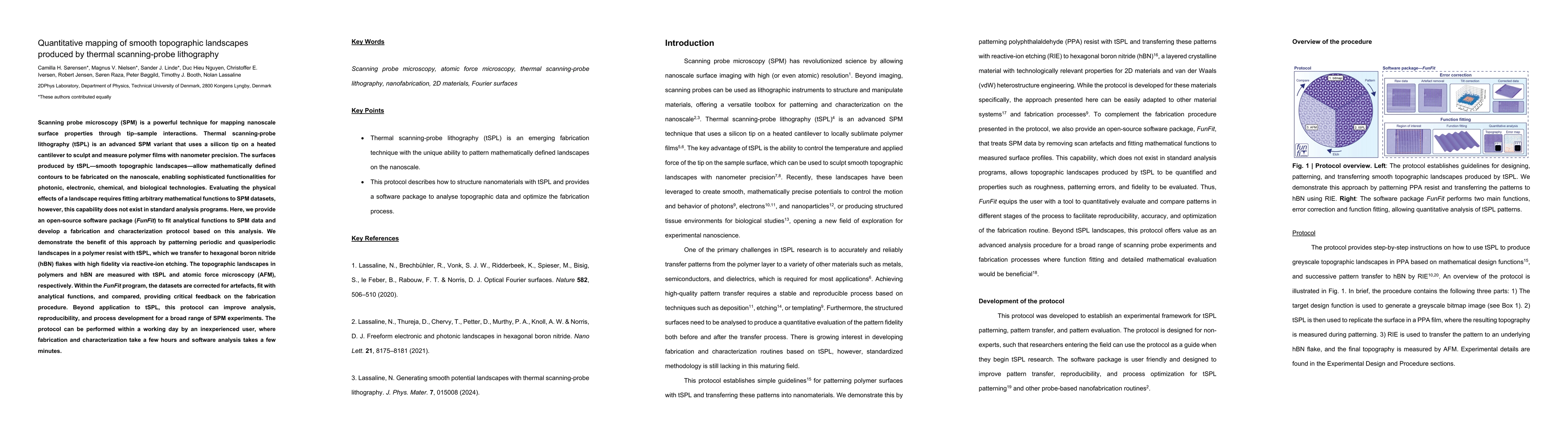
Scanning probe microscopy (SPM) is a powerful technique for mapping nanoscale surface properties through tip-sample interactions. Thermal scanning-probe lithography (tSPL) is an advanced SPM variant t...
Dielectric structures can support low-absorption optical modes, which are attractive for engineering light-matter interactions with excitonic resonances in two-dimensional (2D) materials. However, the...
Two-dimensional (2D) materials such as graphene and hexagonal boron nitride (hBN) provide a versatile platform for quantum electronics. Experiments generally require encapsulating graphene within hBN ...
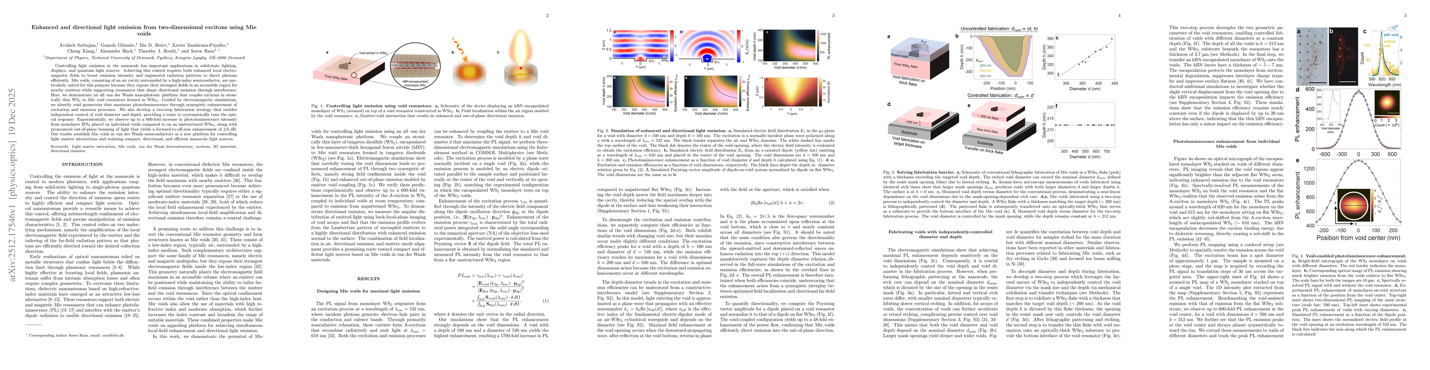
Controlling light emission at the nanoscale has important applications in solid-state lighting, displays, and quantum light sources. Achieving this control requires both enhanced local electromagnetic...