Academic Profile
Statistics
Similar Authors
Papers on arXiv
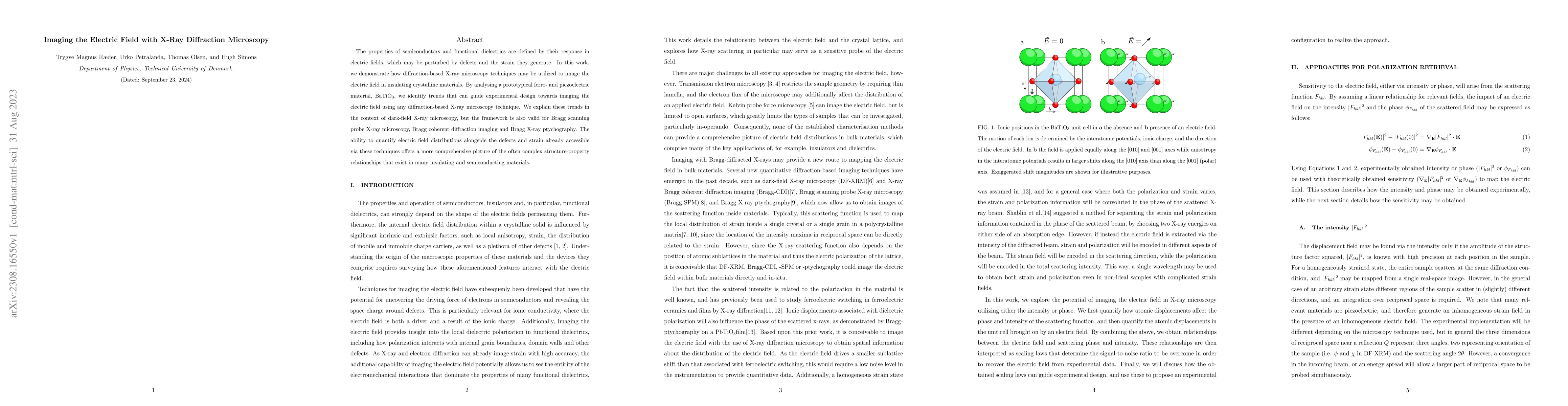
The properties of semiconductors and functional dielectrics are defined by their response in electric fields, which may be perturbed by defects and the strain they generate. In this work, we demonst...
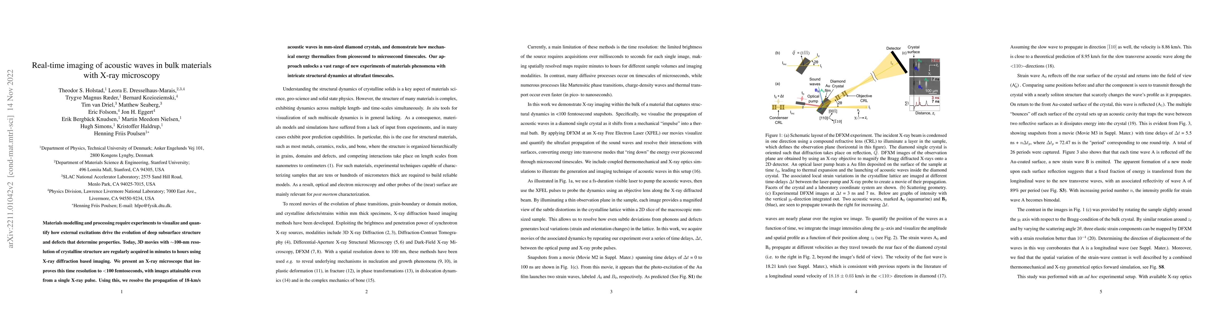
Materials modelling and processing require experiments to visualize and quantify how external excitations drive the evolution of deep subsurface structure and defects that determine properties. Toda...
The structures, strain fields, and defect distributions in solid materials underlie the mechanical and physical properties across numerous applications. Many modern microstructural microscopy tools ...