ArxivLens
U
Researcher

Ulrich Kentsch

16 papers on arXiv

16 arXiv Papers
10 Total Publications
Profile

Academic Profile

Name U. Kentsch
Total Papers 10
Scholar Profile View on Semantic Scholar
Metrics

Statistics

16 arXiv Papers
10 Total Publications
Publications

Papers on arXiv

Thumbnail for Si1-x-yGeySnx alloy formation by Sn ion implantation and flash lamp
  annealing
arXiv
Si1-x-yGeySnx alloy formation by Sn ion implantation and flash lamp annealing

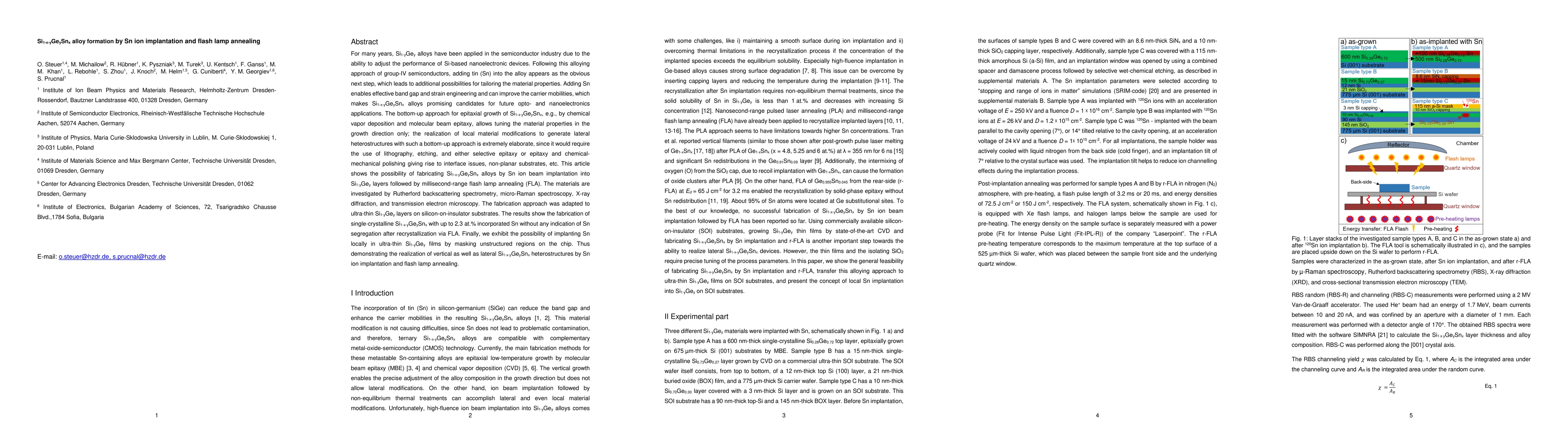
For many years, Si1-yGey alloys have been applied in the semiconductor industry due to the ability to adjust the performance of Si-based nanoelectronic devices. Following this alloying approach of g...

Thumbnail for Extending the coherence time of spin defects in hBN enables advanced
  qubit control and quantum sensing
arXiv
Extending the coherence time of spin defects in hBN enables advanced qubit control and quantum sensing

Spin defects in hexagonal Boron Nitride (hBN) attract increasing interest for quantum technology since they represent optically-addressable qubits in a van der Waals material. In particular, negativ...

Thumbnail for Tripling energy storage density through order-disorder transition
  induced polar nanoregions in PbZrO3 thin films by ion implantation
arXiv
Tripling energy storage density through order-disorder transition induced polar nanoregions in PbZrO3 thin films by ion implantation

Dielectric capacitors are widely used in pulsed power electronic devices due to their ultrahigh power densities and extremely fast charge/discharge speed. To achieve enhanced energy storage density,...

Thumbnail for Emitter-Optomechanical Interaction in Ultra-High-Q hBN Nanocavities
arXiv
Emitter-Optomechanical Interaction in Ultra-High-Q hBN Nanocavities

Integrating quantum emitters into nanocavities which simultaneously couple to the photonic and mechanical modes is critical for interfacing electron spins, photons and phonons in the cavity QED syst...

Thumbnail for Unveiling the Zero-Phonon Line of the Boron Vacancy Center by Cavity
  Enhanced Emission
arXiv
Unveiling the Zero-Phonon Line of the Boron Vacancy Center by Cavity Enhanced Emission

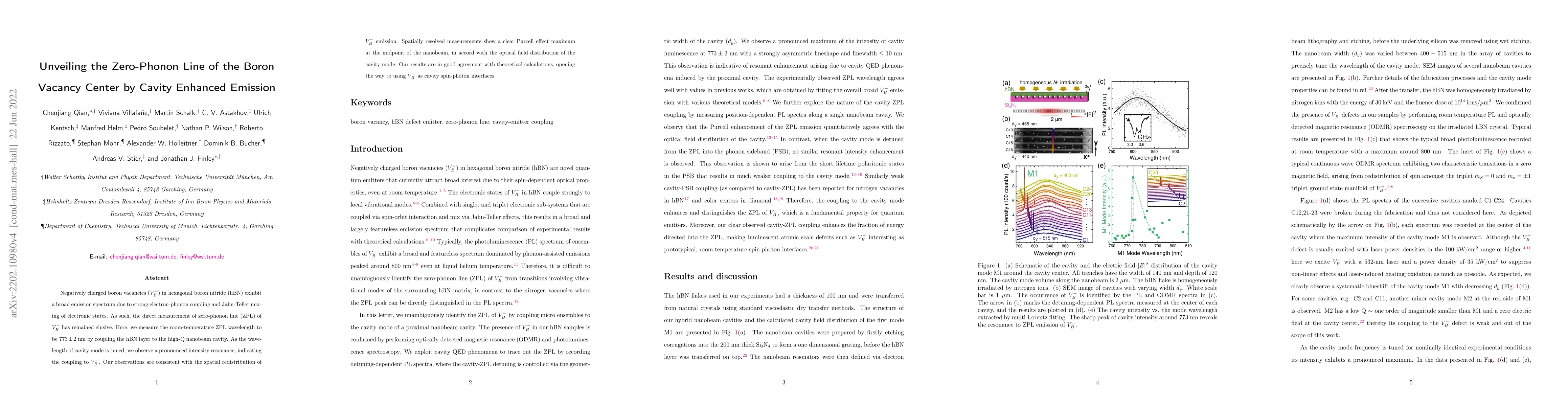
Negatively charged boron vacancies ($V_B^-$) in hexagonal boron nitride (hBN) exhibit a broad emission spectrum due to strong electron-phonon coupling and Jahn-Teller mixing of electronic states. As...

Thumbnail for A photonic platform hosting telecom photon emitters in silicon
arXiv
A photonic platform hosting telecom photon emitters in silicon

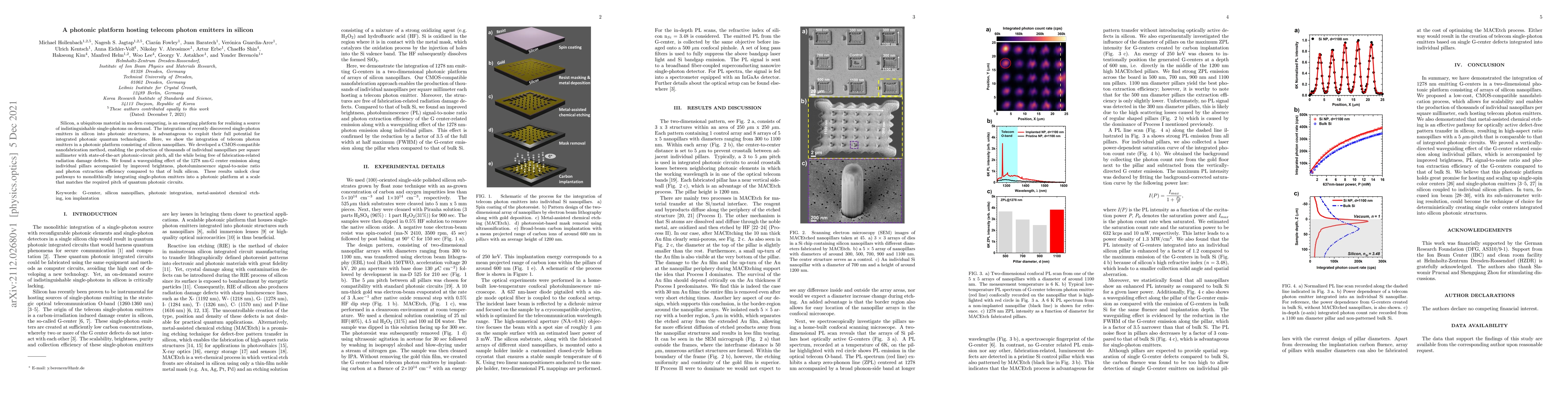
Silicon, a ubiquitous material in modern computing, is an emerging platform for realizing a source of indistinguishable single-photons on demand. The integration of recently discovered single-photon...

Thumbnail for Chlorine doping of MoSe2 flakes by ion implantation
arXiv
Chlorine doping of MoSe2 flakes by ion implantation

The efficient integration of transition metal dichalcogenides (TMDs) into the current electronic device technology requires mastering the techniques of effective tuning of their optoelectronic prope...

Thumbnail for Topological Hall effect in single thick SrRuO3 layers induced by defect
  engineering
arXiv
Topological Hall effect in single thick SrRuO3 layers induced by defect engineering

The topological Hall effect (THE) has been discovered in ultrathin SrRuO3 (SRO) films, where the interface between the SRO layer and another oxide layer breaks the inversion symmetry resulting in th...

Thumbnail for Tuning the metal-insulator transition in epitaxial SrVO3 films by
  uniaxial strain
arXiv
Tuning the metal-insulator transition in epitaxial SrVO3 films by uniaxial strain

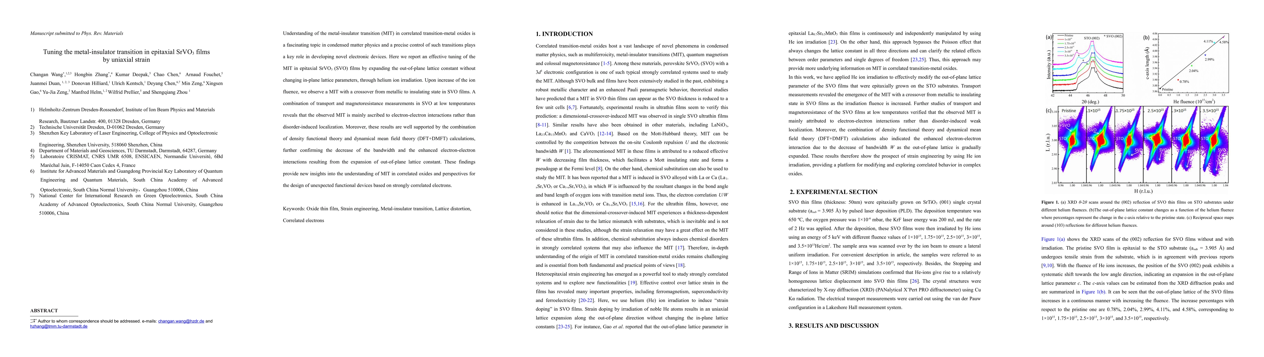
Understanding of the metal-insulator transition (MIT) in correlated transition-metal oxides is a fascinating topic in condensed matter physics and a precise control of such transitions plays a key r...

Thumbnail for Photon emission gain in Er doped Si light emitting diodes by impact
  excitation
arXiv
Photon emission gain in Er doped Si light emitting diodes by impact excitation

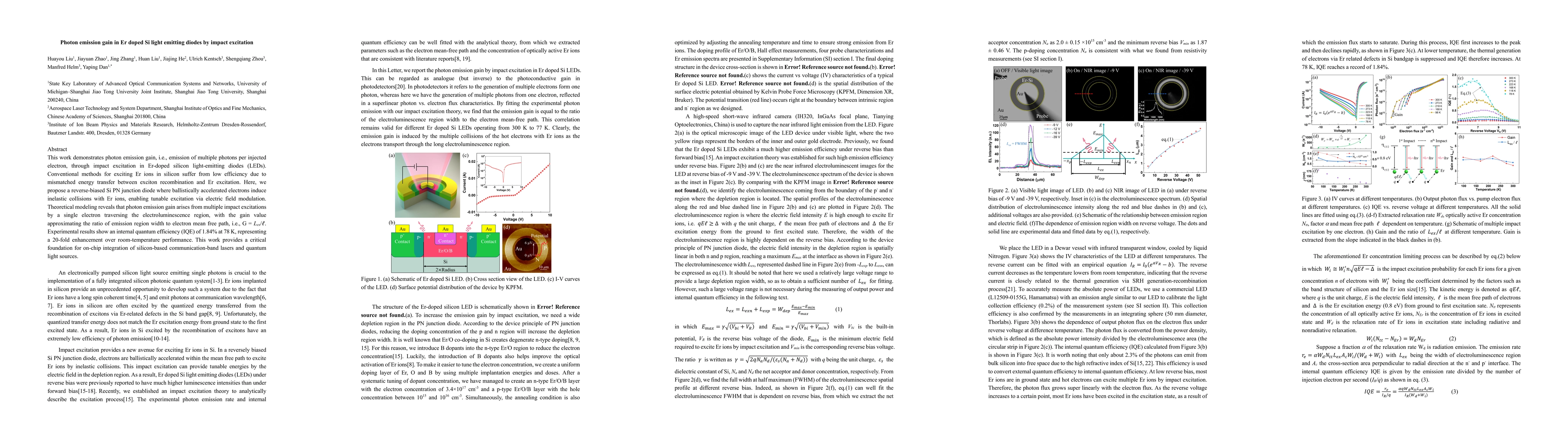
This work demonstrates photon emission gain, i.e., emission of multiple photons per injected electron, through impact excitation in Er-doped silicon light-emitting diodes (LEDs). Conventional methods ...

Thumbnail for Highly Enhanced robust room temperature ferromagnetism in CVD-grown
  nano-dimensional MoS2 flakes by modifying edges and defect engineering
arXiv
Highly Enhanced robust room temperature ferromagnetism in CVD-grown nano-dimensional MoS2 flakes by modifying edges and defect engineering

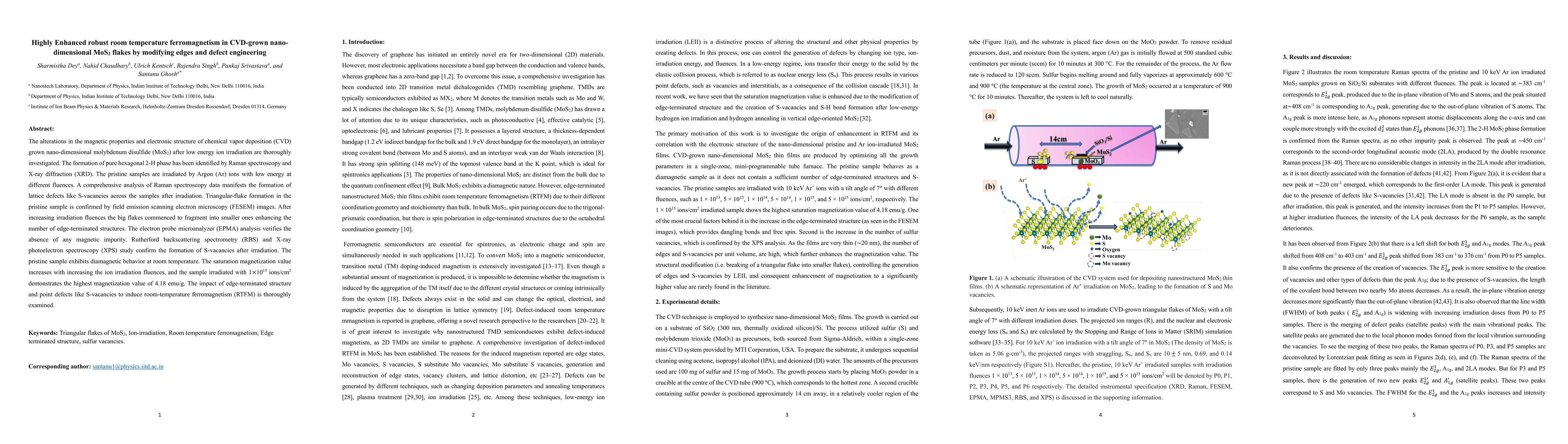
The alterations in the magnetic properties and electronic structure of chemical vapor deposition (CVD) grown nano-dimensional molybdenum disulfide (MoS2) after low energy ion irradiation are thoroughl...

Thumbnail for Structural and Optical Properties of Crystal Ion Sliced BaTiO$_3$ Thin
  Films
arXiv
Structural and Optical Properties of Crystal Ion Sliced BaTiO$_3$ Thin Films

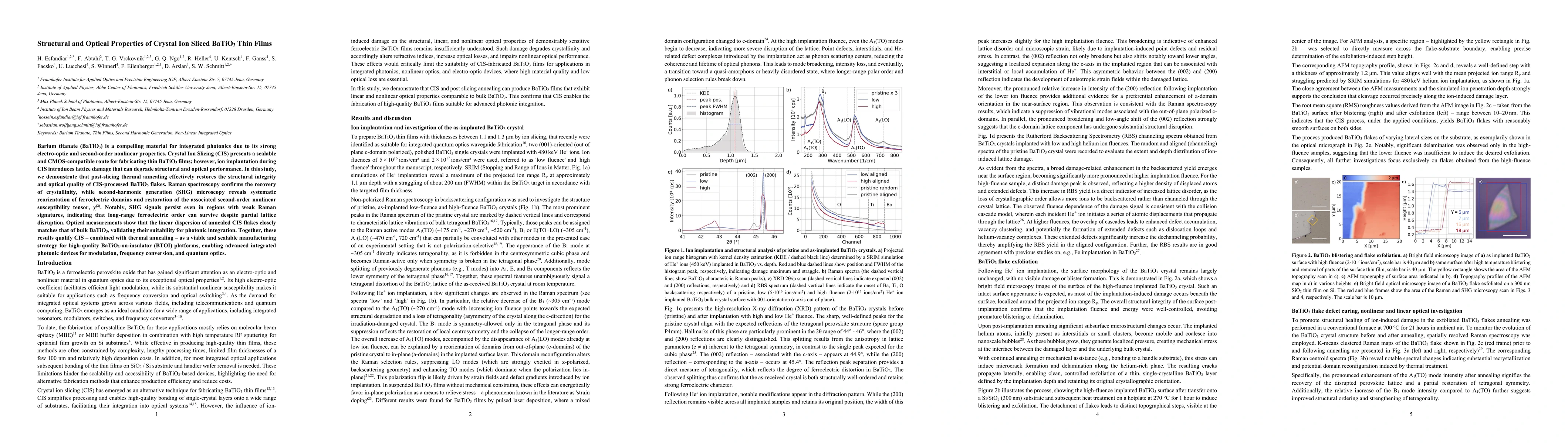
Barium titanate (BaTiO$_3$) is a compelling material for integrated photonics due to its strong electro-optic and second-order nonlinear properties. Crystal Ion Slicing (CIS) presents a scalable and C...

Thumbnail for High-pulse-energy integrated mode-locked lasers based on a Mamyshev
  oscillator
arXiv
High-pulse-energy integrated mode-locked lasers based on a Mamyshev oscillator

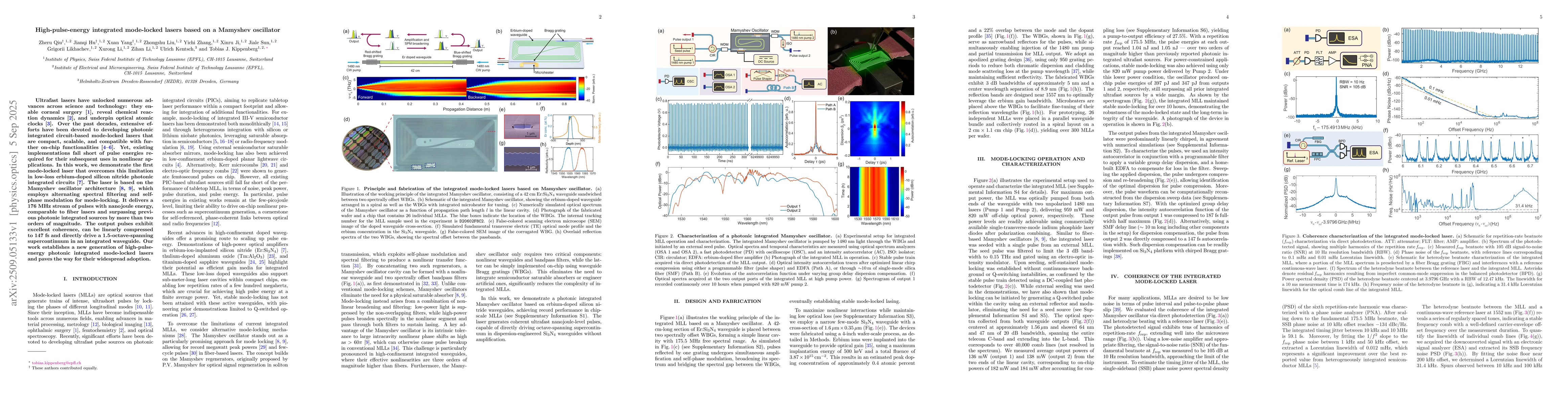
Ultrafast lasers have unlocked numerous advances across science and technology: they enable corneal surgery, reveal chemical reaction dynamics, and underpin optical atomic clocks. Over the past decade...

Thumbnail for Structural and Optical Characteristics of beta-Ga2O3 Implanted with Rare Earth Ions
arXiv
Structural and Optical Characteristics of beta-Ga2O3 Implanted with Rare Earth Ions

We investigated the structural evolution and optical properties of beta-Ga2O3 crystals implanted with different rare-earth (RE) ions using channeling Rutherford Backscattering Spectrometry, Positron A...

Thumbnail for Comprehensive structural and optical analysis of differently oriented Yb-implanted $β$-Ga$_2$O$_3$
arXiv
Comprehensive structural and optical analysis of differently oriented Yb-implanted $β$-Ga$_2$O$_3$

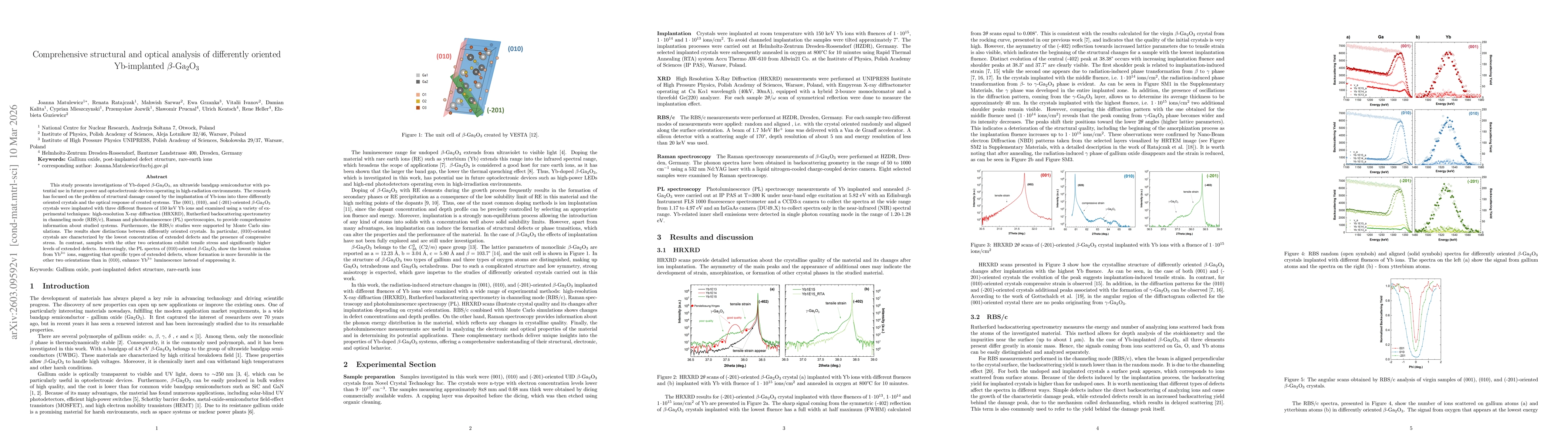
This study presents investigations of Yb-doped $β$-Ga$_2$O$_3$, an ultrawide bandgap semiconductor with potential use in future power and optoelectronic devices operating in high-radiation environment...

Thumbnail for Tailoring the properties of YBa$_{2}$Cu$_{3}$O$_{7-δ}$ thin films by 30 keV He$^+$ irradiation: An enabling route to superconducting device nanopatterning
arXiv
Tailoring the properties of YBa$_{2}$Cu$_{3}$O$_{7-δ}$ thin films by 30 keV He$^+$ irradiation: An enabling route to superconducting device nanopatterning

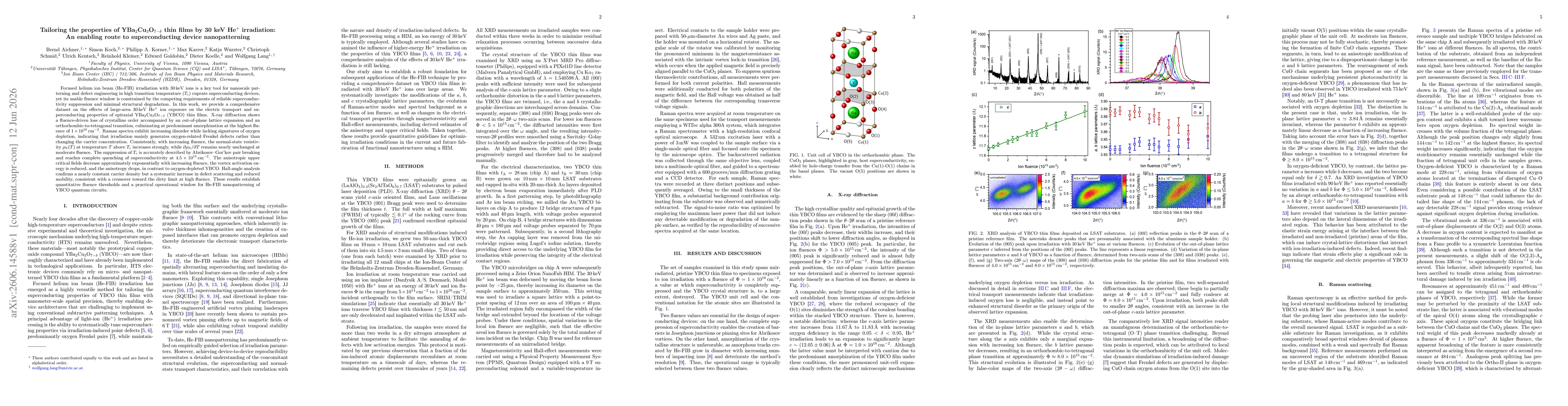
Focused helium ion beam (He-FIB) irradiation with 30 keV ions is a key tool for nanoscale patterning and defect engineering in high transition temperature (Tc) cuprate superconducting devices, yet its...

This website uses cookies to ensure you get the best experience. Learn more