Academic Profile
Statistics
Similar Authors
Papers on arXiv
Achieving stable, high-quality quantum dots has proven challenging within device architectures rooted in conventional solid-state device fabrication paradigms. In fact, these are grappled with compl...
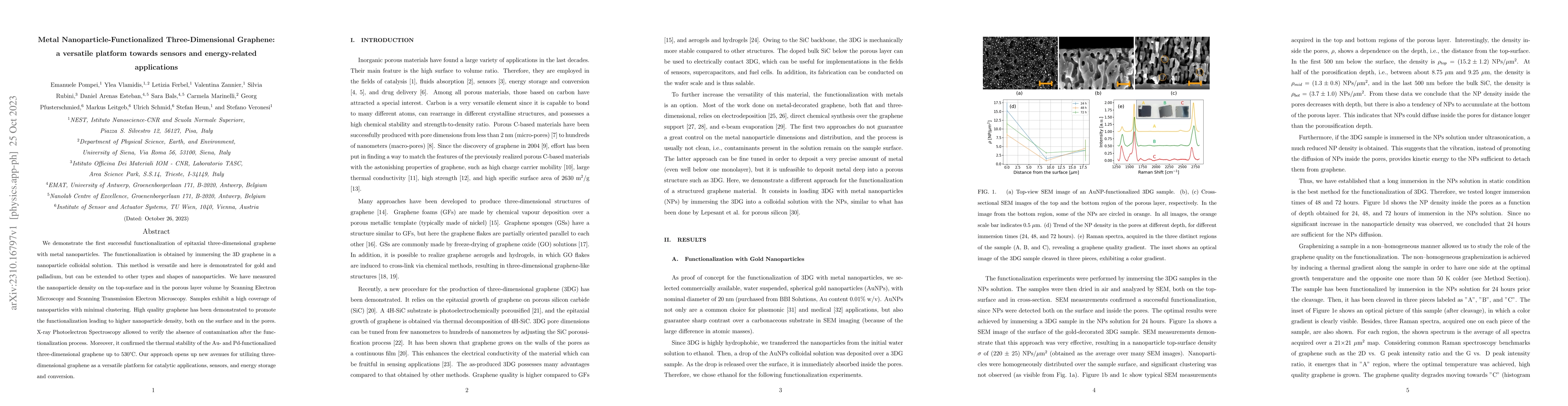
We demonstrate the first successful functionalization of epitaxial three-dimensional graphene with metal nanoparticles. The functionalization is obtained by immersing the 3D graphene in a nanopartic...
The possibility to tune the functional properties of nanomaterials is key to their technological applications. Superlattices, i.e., periodic repetitions of two or more materials in different dimensi...
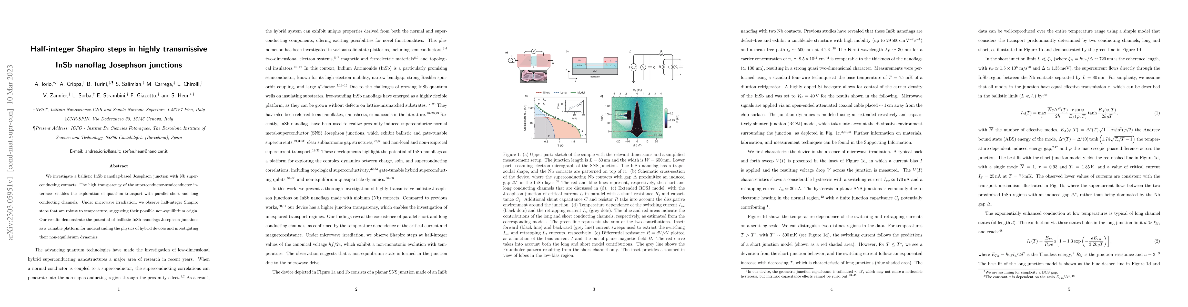
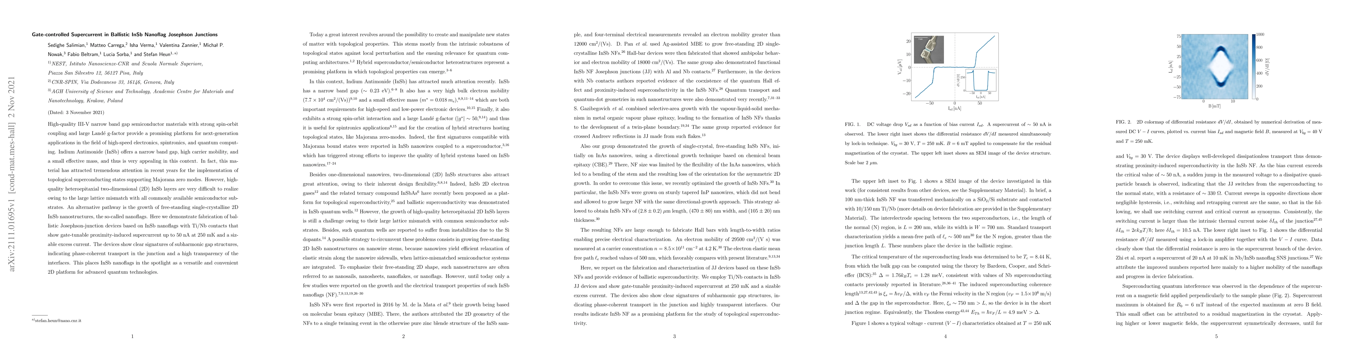
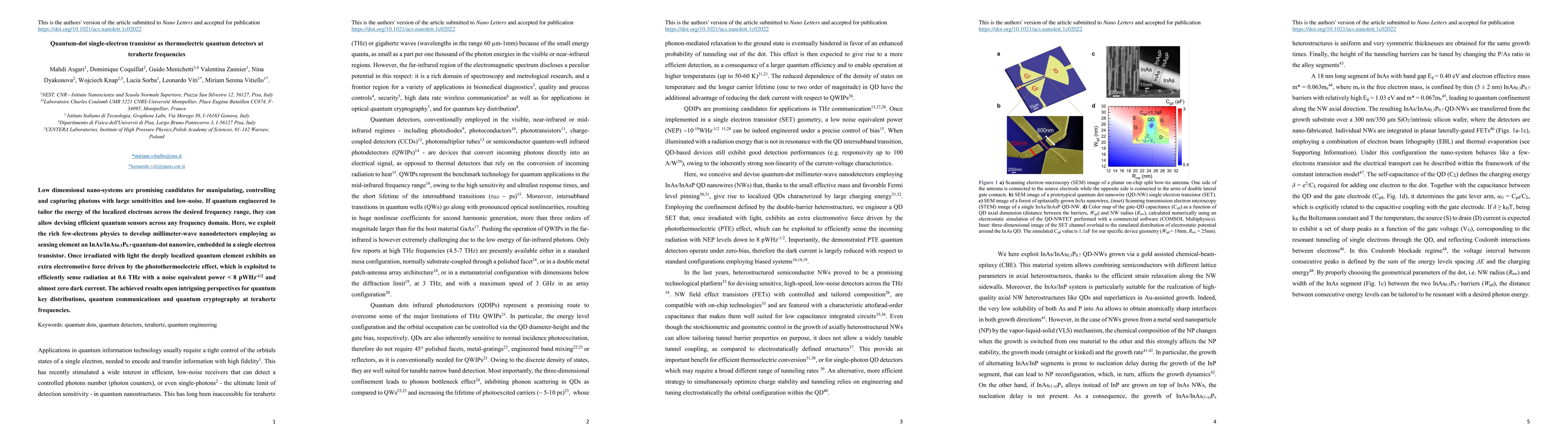
We investigate a ballistic InSb nanoflag-based Josephson junction with Nb superconducting contacts. The high transparency of the superconductor-semiconductor interfaces enables the exploration of qu...
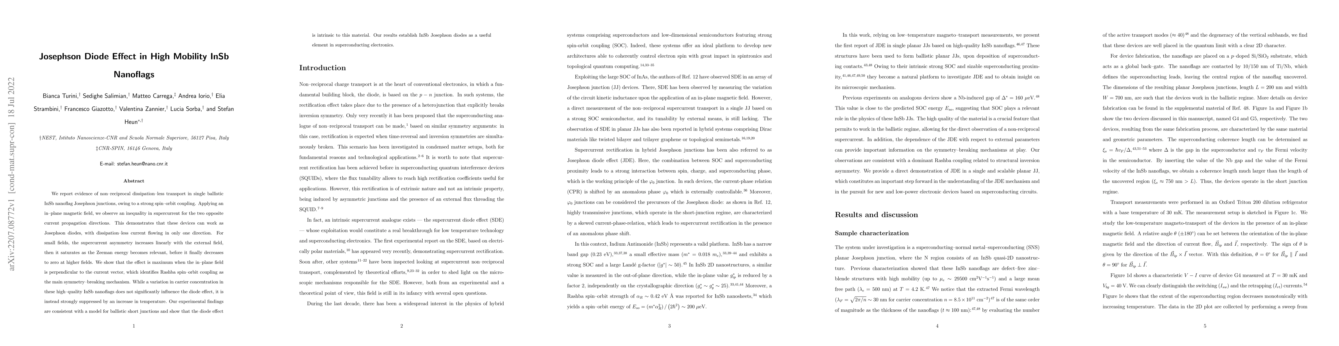
We report evidence of non-reciprocal dissipation-less transport in single ballistic InSb nanoflag Josephson junctions, owing to a strong spin-orbit coupling. Applying an in-plane magnetic field, we ...
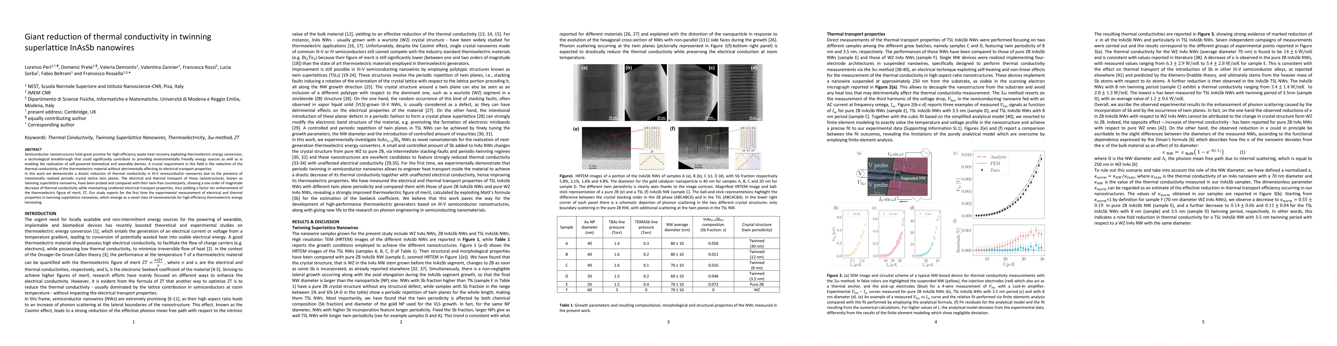
Semiconductor nanostructures hold great promise for high-efficiency waste heat recovery exploiting thermoelectric energy conversion, a technological breakthrough that could significantly contribute ...
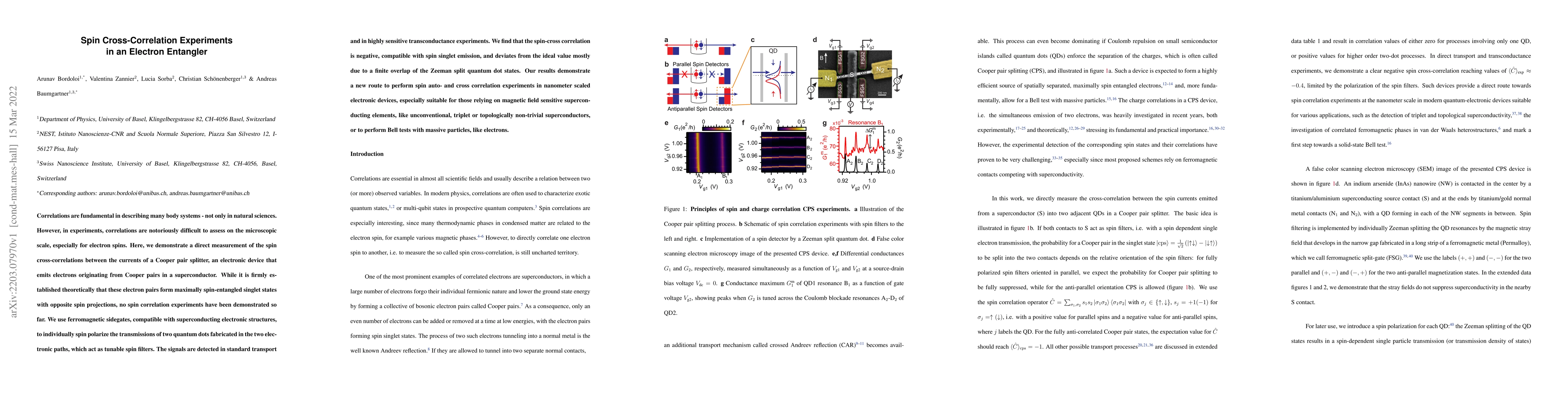
Correlations are fundamental in describing many body systems - not only in natural sciences. However, in experiments, correlations are notoriously difficult to assess on the microscopic scale, espec...
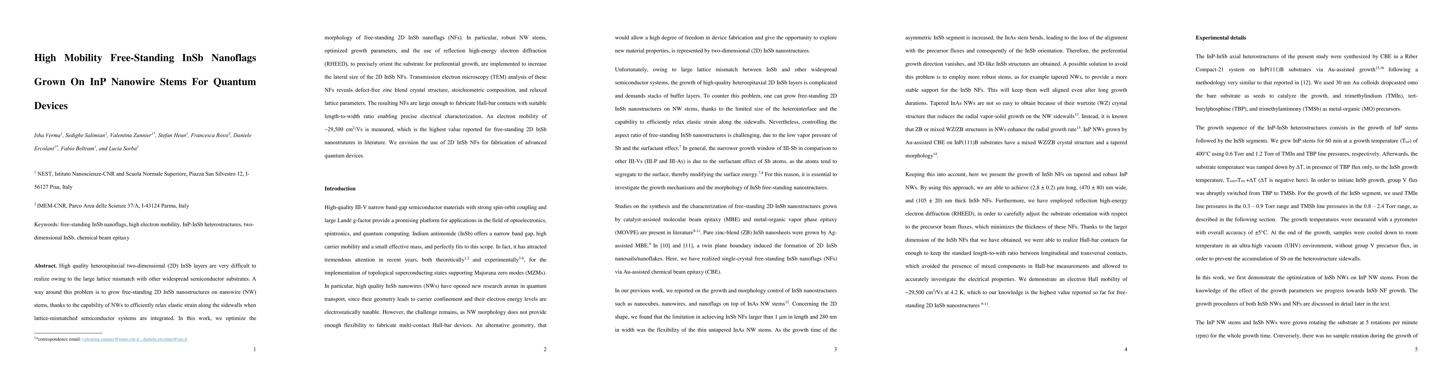
High quality heteroepitaxial two-dimensional (2D) InSb layers are very difficult to realize owing to the large lattice mismatch with other widespread semiconductor substrates. A way around this prob...
High-quality III-V narrow band gap semiconductor materials with strong spin-orbit coupling and large Lande g-factor provide a promising platform for next-generation applications in the field of high...
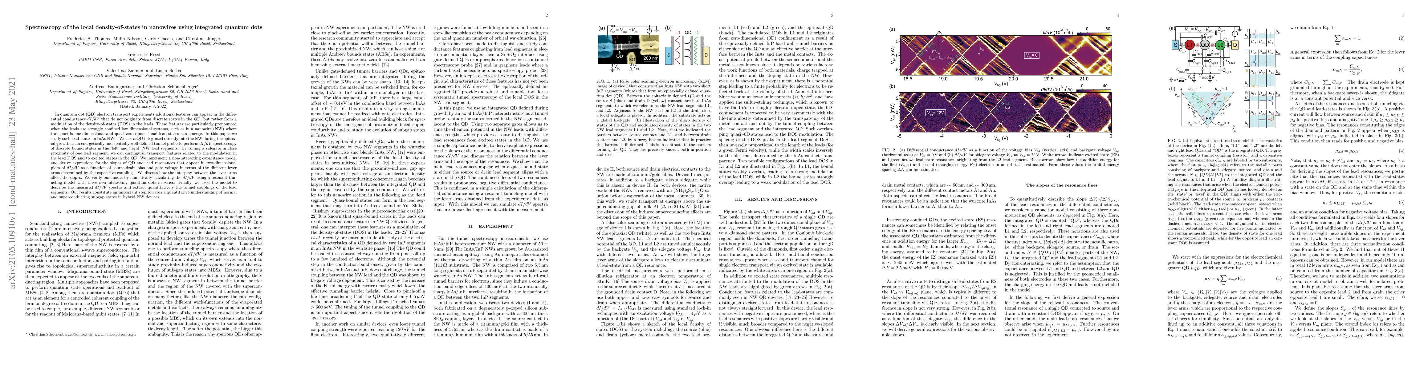
Low dimensional nano-systems are promising candidates for manipulating, controlling and capturing photons with large sensitivities and low-noise. If quantum engineered to tailor the energy of the lo...
In quantum dot (QD) electron transport experiments additional features can appear in the differential conductance $dI/dV$ that do not originate from discrete states in the QD, but rather from a modu...
The combination of core/shell geometry and band gap engineering in nanowire heterostructures can be employed to realize systems with novel transport and optical properties. Here, we report on the gr...
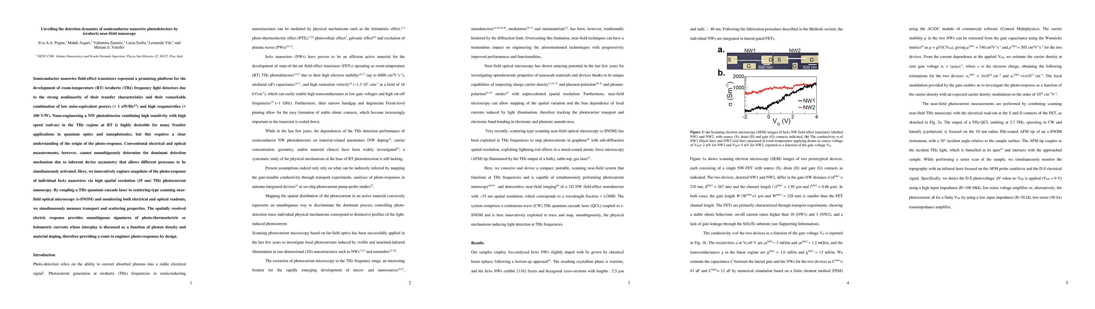
Semiconductor nanowire field-effect transistors represent a promising platform for the development of room-temperature (RT) terahertz (THz) frequency light detectors due to the strong nonlinearity o...
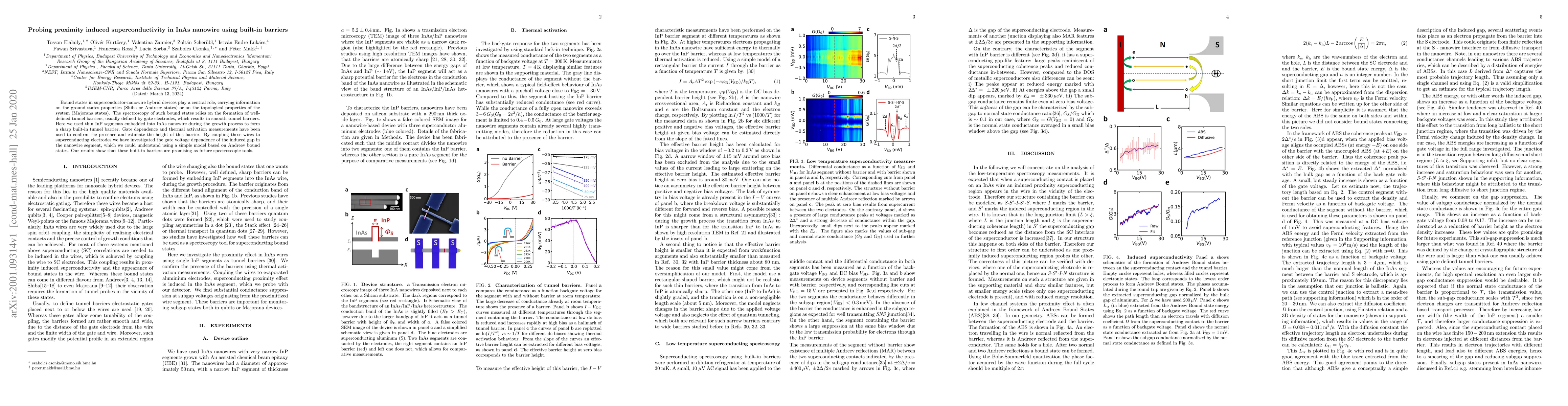
Bound states in superconductor-nanowire hybrid devices play a central role, carrying informationon the ground states properties (Shiba or Andreev states) or on the topological properties of thesyste...
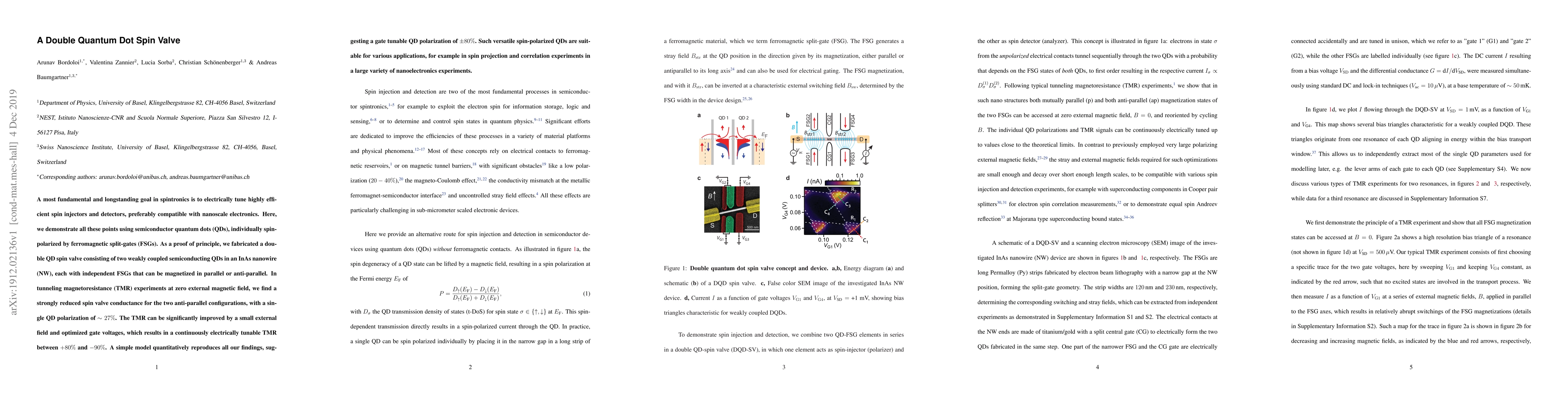
A most fundamental and longstanding goal in spintronics is to electrically tune highly efficient spin injectors and detectors, preferably compatible with nanoscale electronics. Here, we demonstrate ...
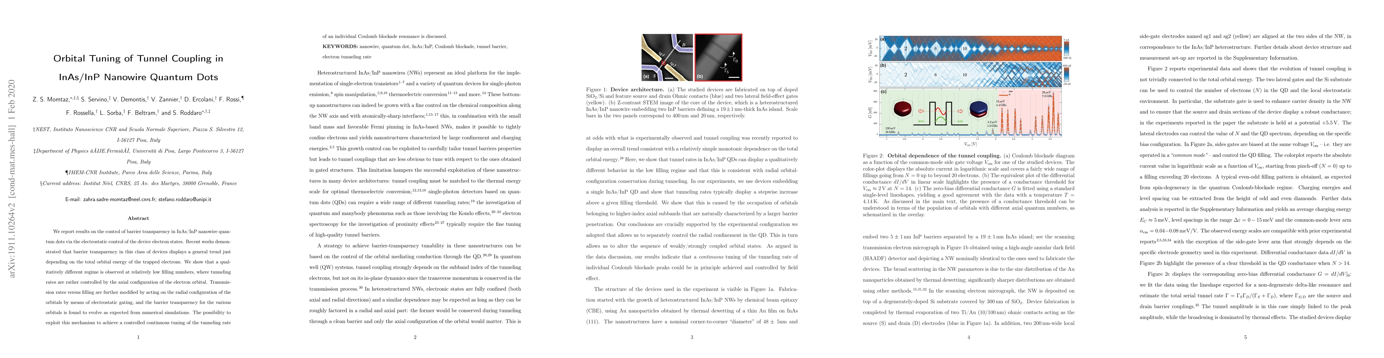
We report results on the control of barrier transparency in InAs/InP nanowire quantum dots via the electrostatic control of the device electron states. Recent works demonstrated that barrier transpa...
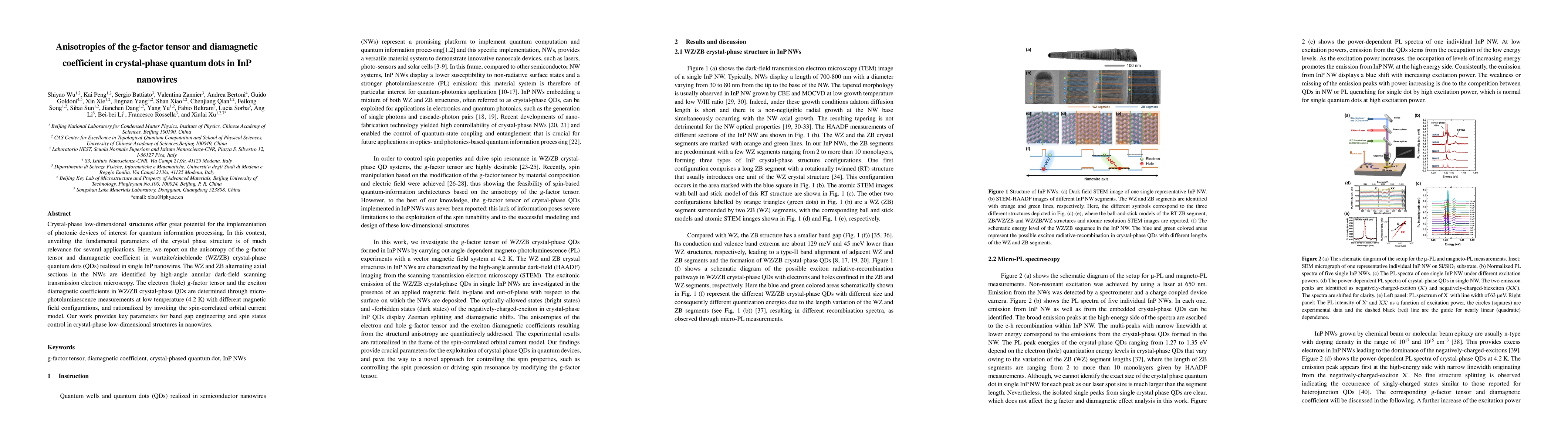
Crystal-phase low-dimensional structures offer great potential for the implementation of photonic devices of interest for quantum information processing. In this context, unveiling the fundamental p...
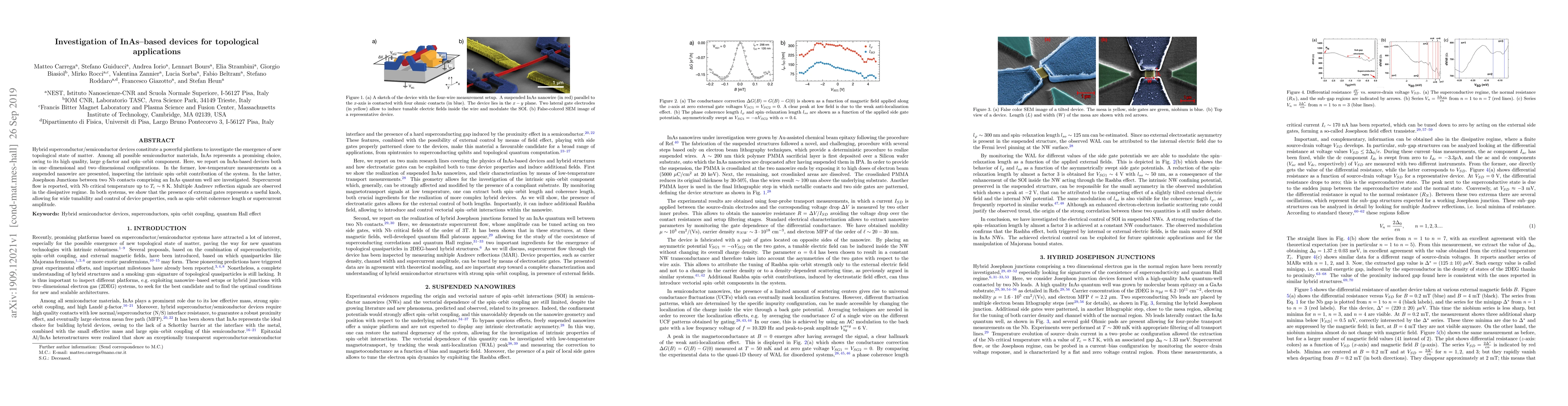
Hybrid superconductor/semiconductor devices constitute a powerful platform to investigate the emergence of new topological state of matter. Among all possible semiconductor materials, InAs represent...
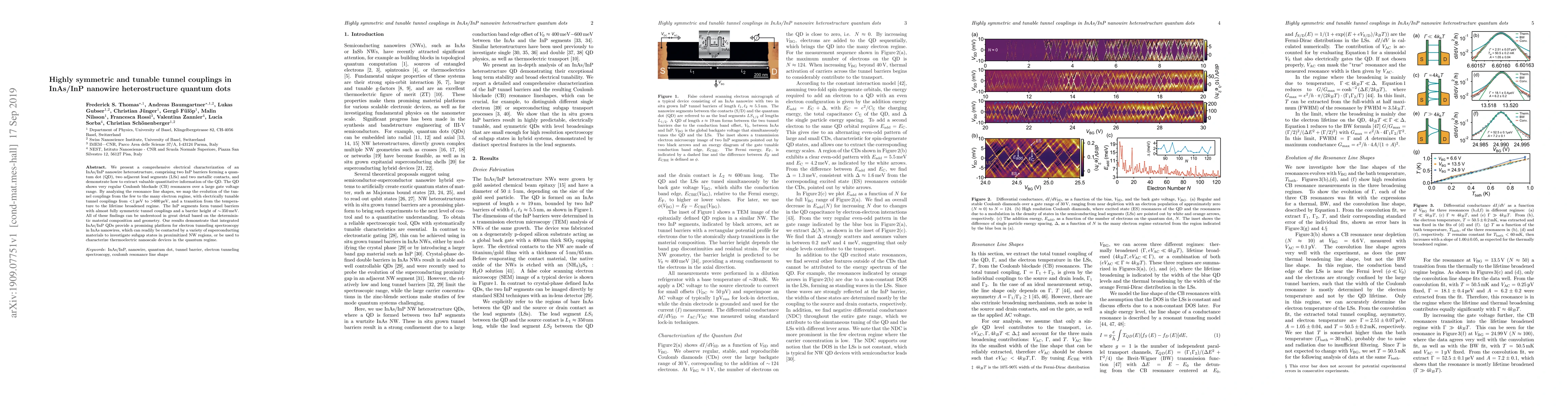
We present a comprehensive electrical characterization of an InAs/InP nanowire heterostructure, comprising two InP barriers forming a quantum dot (QD), two adjacent lead segments (LSs) and two metal...
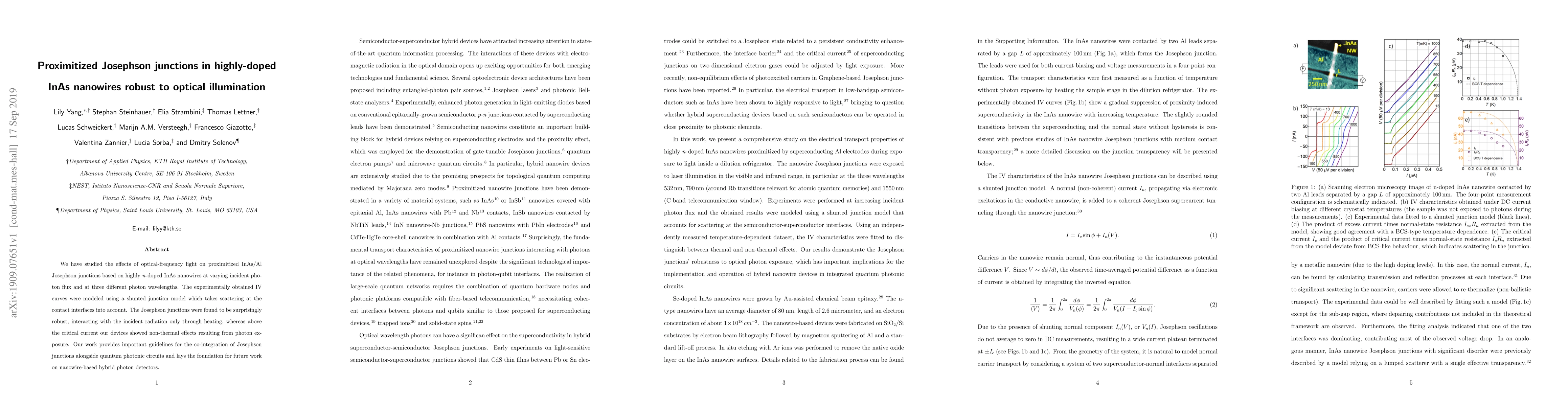
We have studied the effects of optical-frequency light on proximitized InAs/Al Josephson junctions based on highly n-doped InAs nanowires at varying incident photon flux and at three different photo...
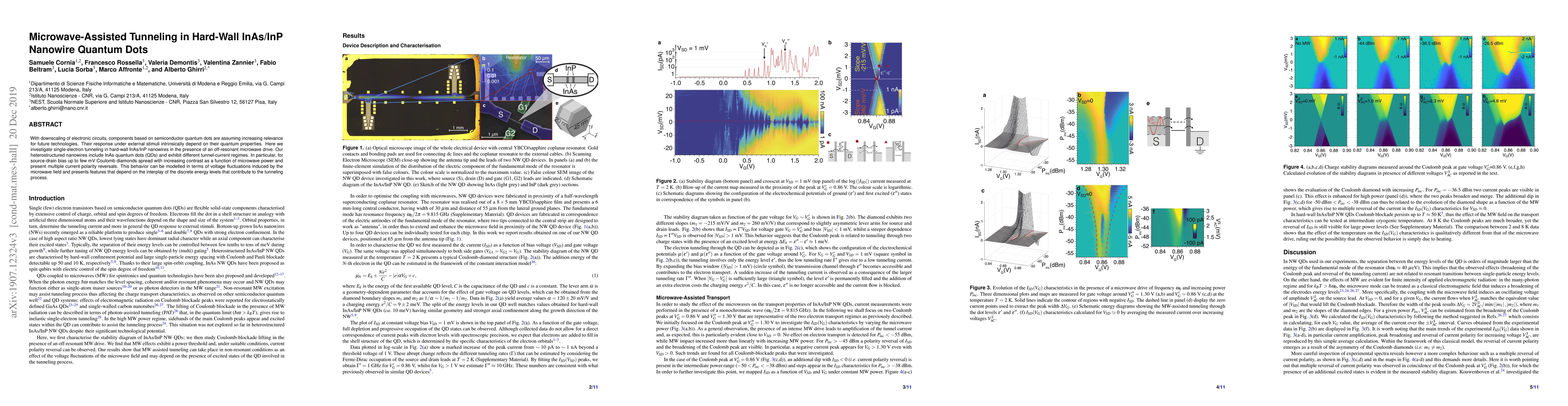
With downscaling of electronic circuits, components based on semiconductor quantum dots are assuming increasing relevance for future technologies. Their response under external stimuli intrinsically...
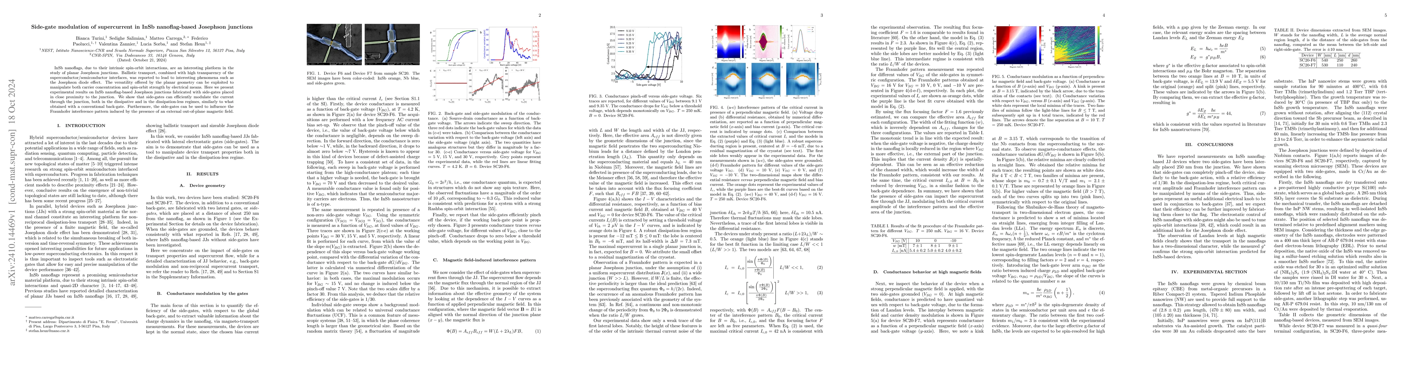
InSb nanoflags, due to their intrinsic spin-orbit interactions, are an interesting platform in the study of planar Josephson junctions. Ballistic transport, combined with high transparency of the supe...
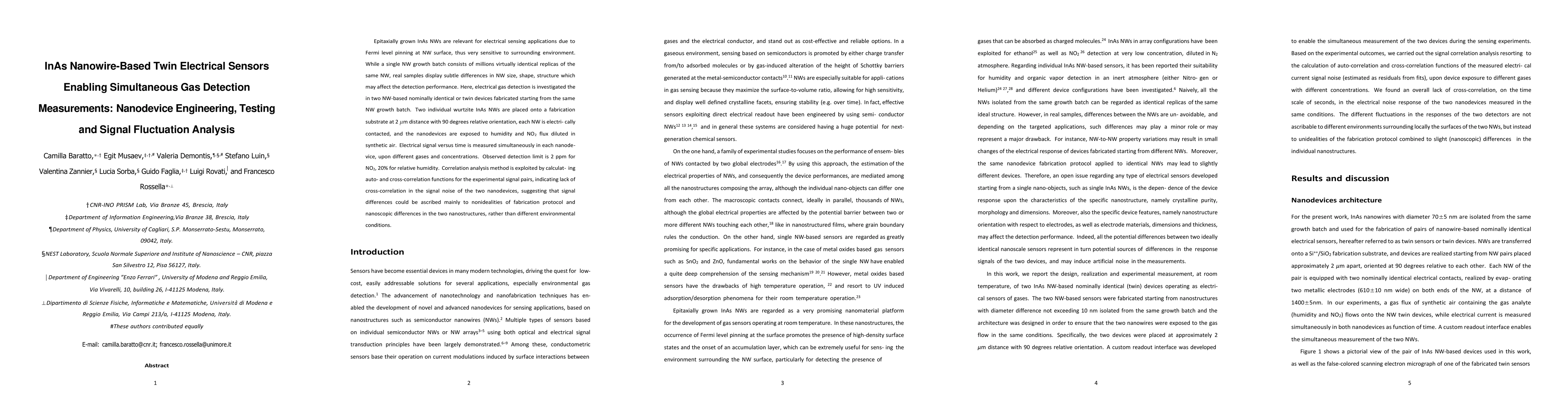
Epitaxially grown InAs NWs are relevant for electrical sensing applications due to Fermi level pinning at NW surface, thus very sensitive to surrounding environment. While a single NW growth batch con...
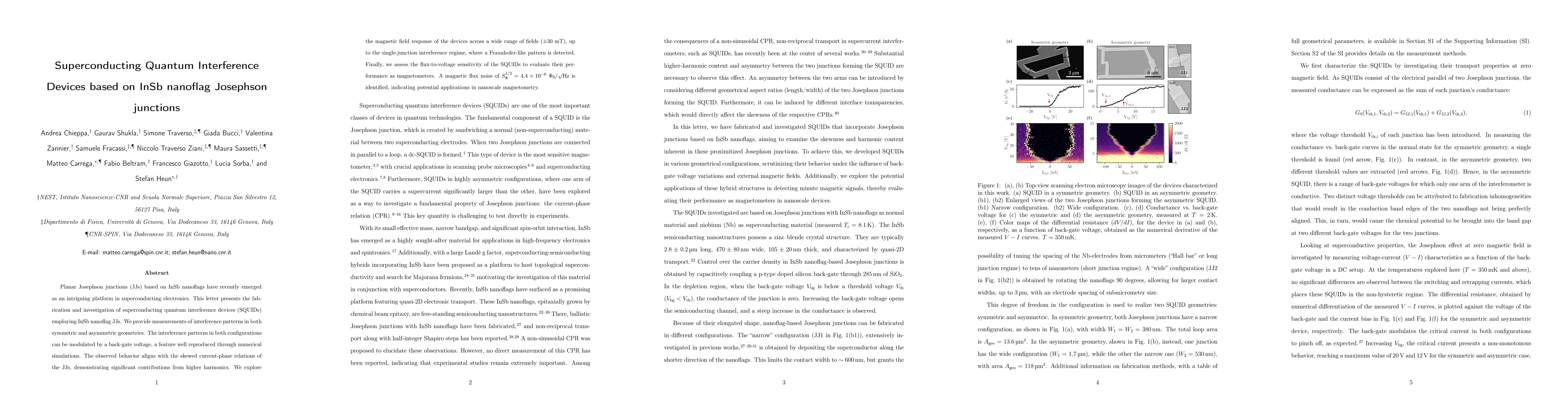
Planar Josephson junctions (JJs) based on InSb nanoflags have recently emerged as an intriguing platform in superconducting electronics. This letter presents the fabrication and investigation of super...
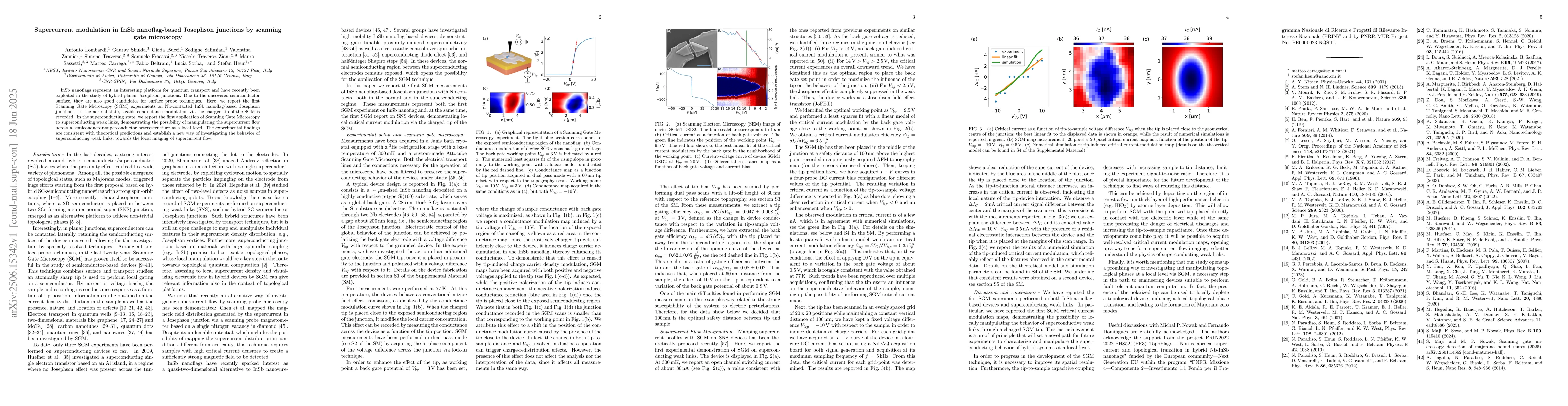
InSb nanoflags represent an interesting platform for quantum transport and have recently been exploited in the study of hybrid planar Josephson junctions. Due to the uncovered semiconductor surface, t...
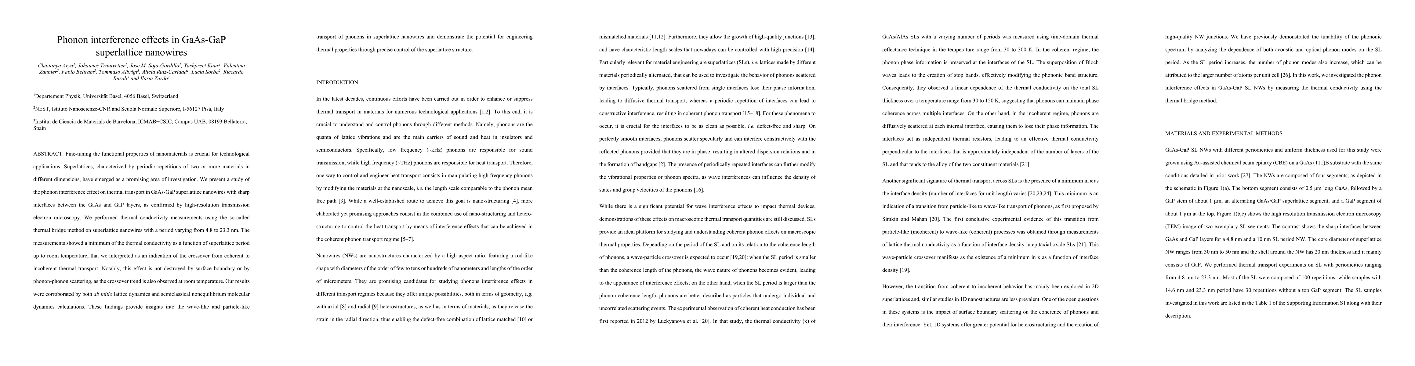
Fine-tuning the functional properties of nanomaterials is crucial for technological applications. Superlattices, characterized by periodic repetitions of two or more materials in different dimensions,...

The present work reports, for the first time, the growth of high-quality free-standing InAsSb nanoflags and their electronic properties. Different growth conditions have been explored, and zinc-blende...
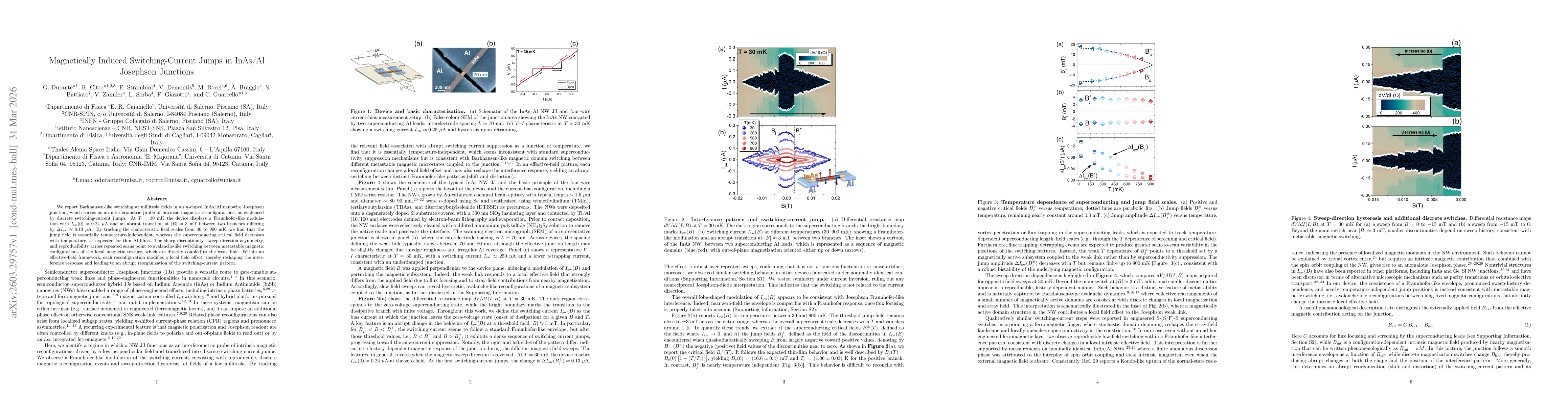
We report Barkhausen-like switching at millitesla fields in an $n$-doped InAs/Al nanowire Josephson junction, which serves as an interferometric probe of intrinsic magnetic reconfigurations, as eviden...