Academic Profile
Statistics
Similar Authors
Papers on arXiv
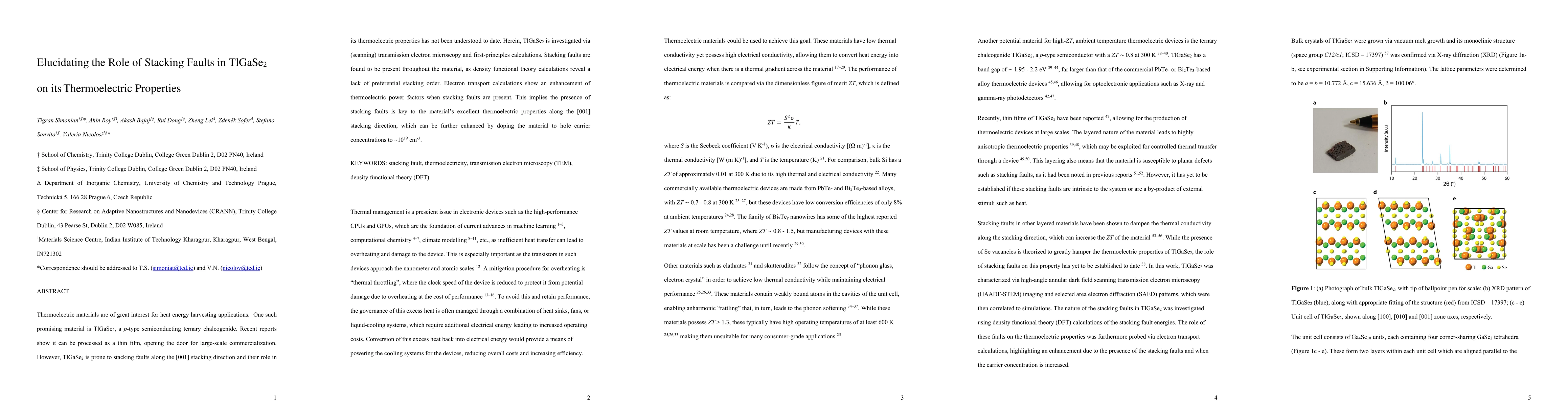
Thermoelectric materials are of great interest for heat energy harvesting applications. One such promising material is TlGaSe$_{2}$, a p-type semiconducting ternary chalcogenide. Recent reports show...
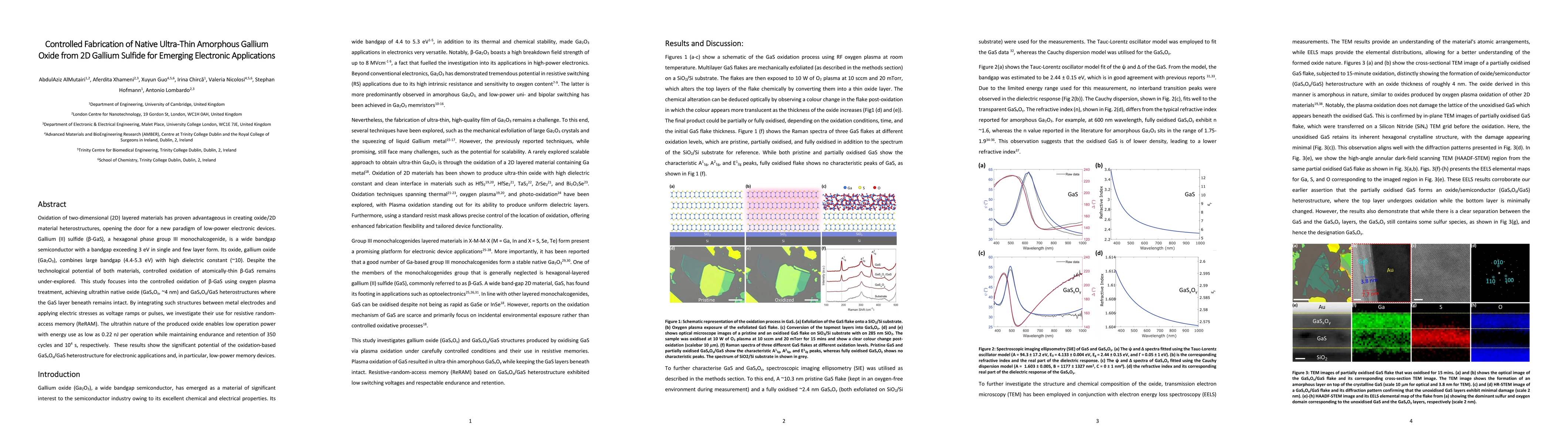
Oxidation of two-dimensional (2D) layered materials has proven advantageous in creating oxide/2D material heterostructures, opening the door for a new paradigm of low-power electronic devices. Galli...
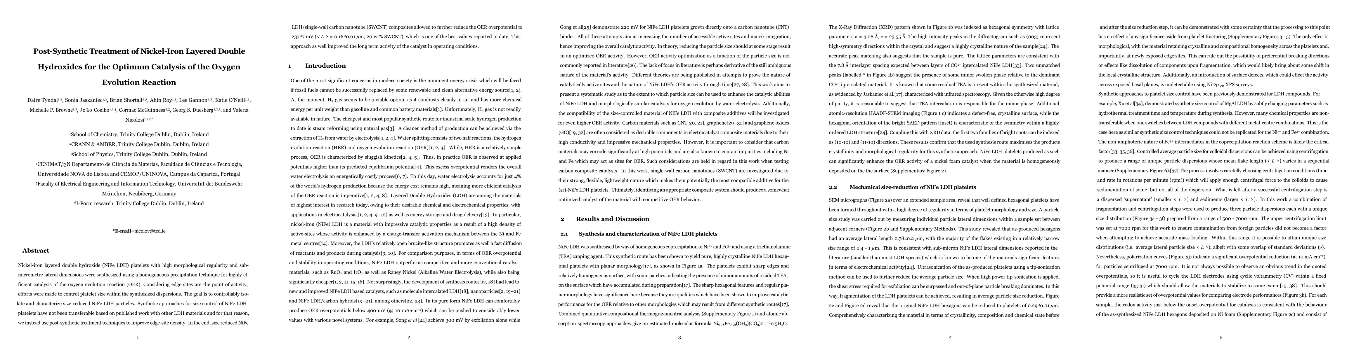
Nickel-iron layered double hydroxide (NiFe LDH) platelets with high morphological regularity and sub-micrometre lateral dimensions were synthesized using a homogeneous precipitation technique for hi...
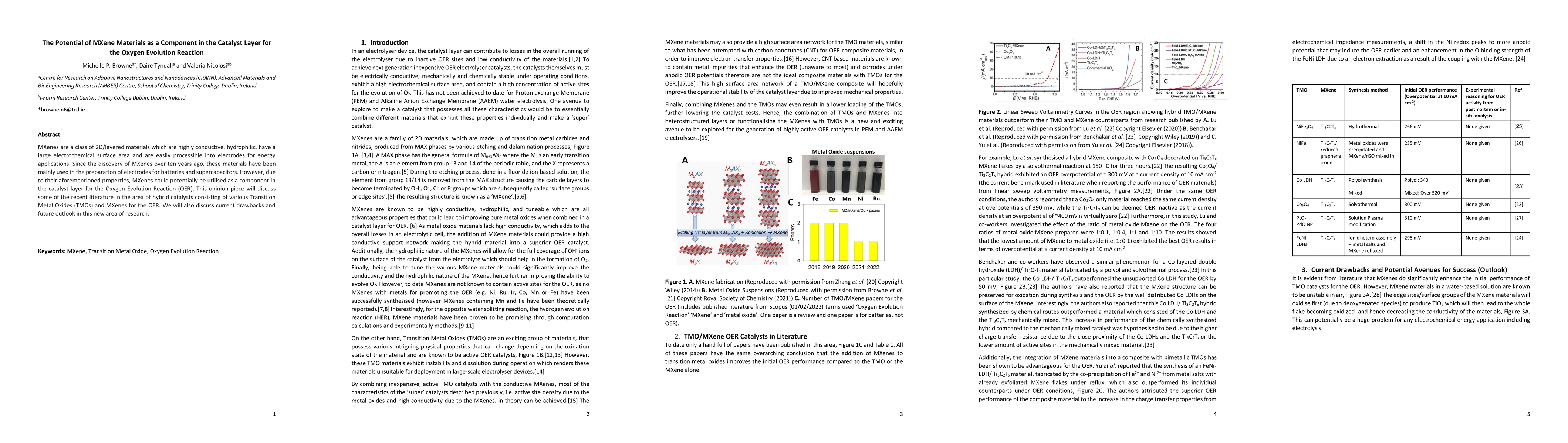
MXenes are a class of 2D/layered materials which are highly conductive, hydrophilic, have a large electrochemical surface area and are easily processible into electrodes for energy applications. Sin...
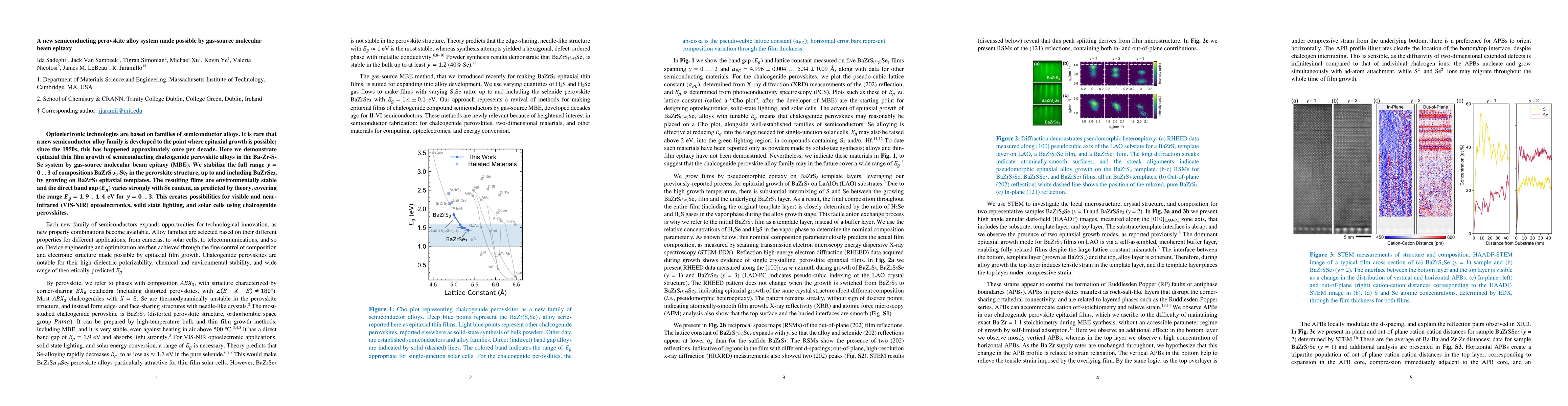
Optoelectronic technologies are based on families of semiconductor alloys. It is rare that a new semiconductor alloy family is developed to the point where epitaxial growth is possible; since the 19...
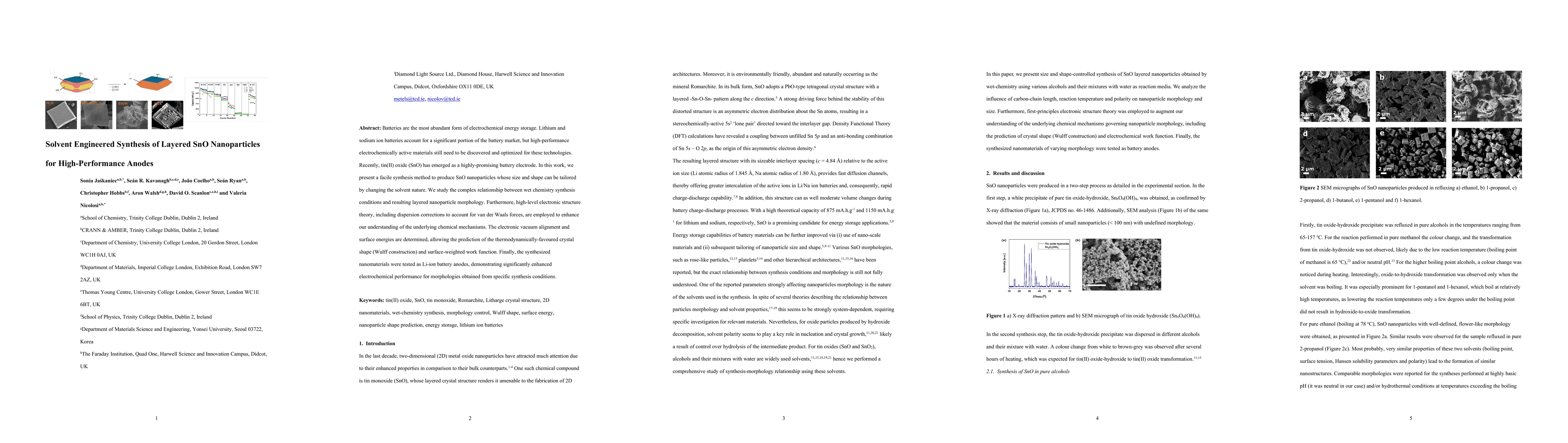
Batteries are the most abundant form of electrochemical energy storage. Lithium and sodium ion batteries account for a significant portion of the battery market, but high-performance electrochemical...
While it is well-known that electrode conductivity has a critical impact on rate-performance in battery electrodes, this relationship has been quantified only by computer simulations. Here we invest...
For battery electrodes, measured capacity decays as charge/discharge current is increased. Such rate-performance is important from a practical perspective and is usually characterised via galvanosta...
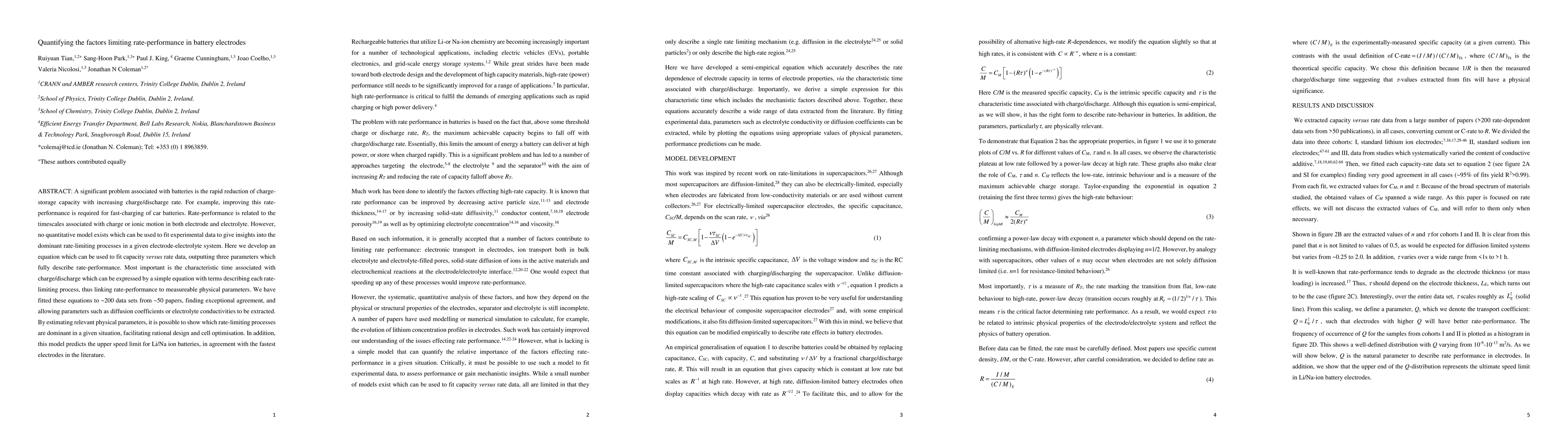
A significant problem associated with batteries is the rapid reduction of charge-storage capacity with increasing charge/discharge rate. For example, improving this rate-performance is required for ...
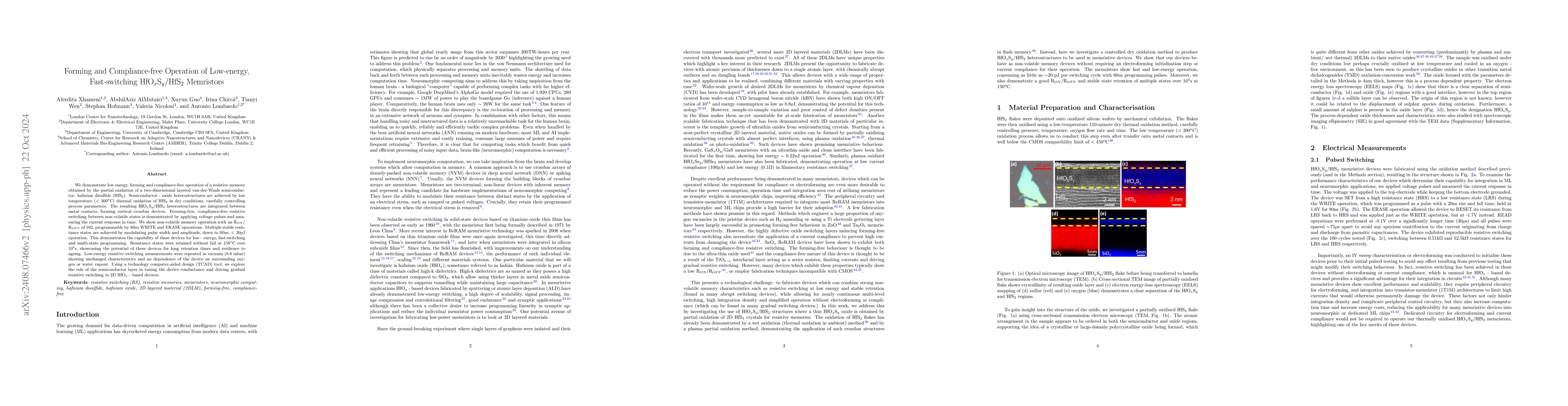
We demonstrate low energy, forming and compliance-free operation of a resistive memory obtained by the partial oxidation of a two-dimensional layered van-der-Waals semiconductor: hafnium disulfide (Hf...
Two-dimensional (2D) transition metal dichalcogenides (TMDCs), exemplified by molybdenum disulfide (MoS2), have shown exceptional potential for data-centred, energy-efficient electronic applications d...
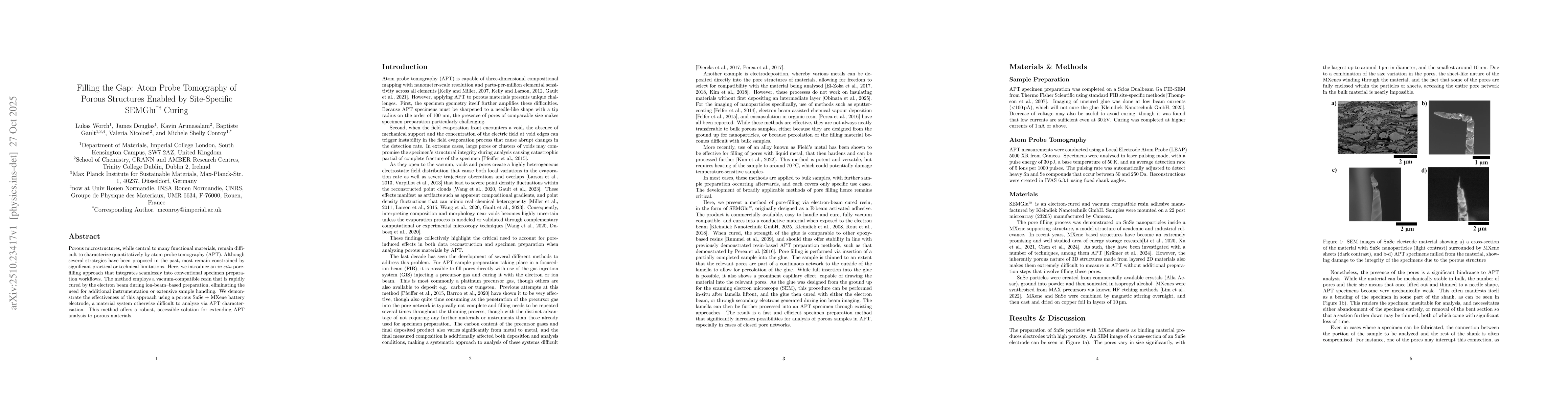
Porous microstructures, while central to many functional materials, remain difficult to characterize quantitatively by atom probe tomography (APT). Although several strategies have been proposed over ...
Understanding degradation processes in lithium ion batteries is essential for improving long term performance and advancing sustainable energy technologies. Tin selenide (SnSe) has emerged as a promis...