Vincent Calvo

5 papers on arXiv

Academic Profile

Name: V. Calvo
Total Papers: 20

Statistics

arXiv Papers 5
Total Publications 20

Papers on arXiv

Thumbnail for Purcell enhancement of silicon W centers in circular Bragg grating
  cavities

Purcell enhancement of silicon W centers in circular Bragg grating cavities

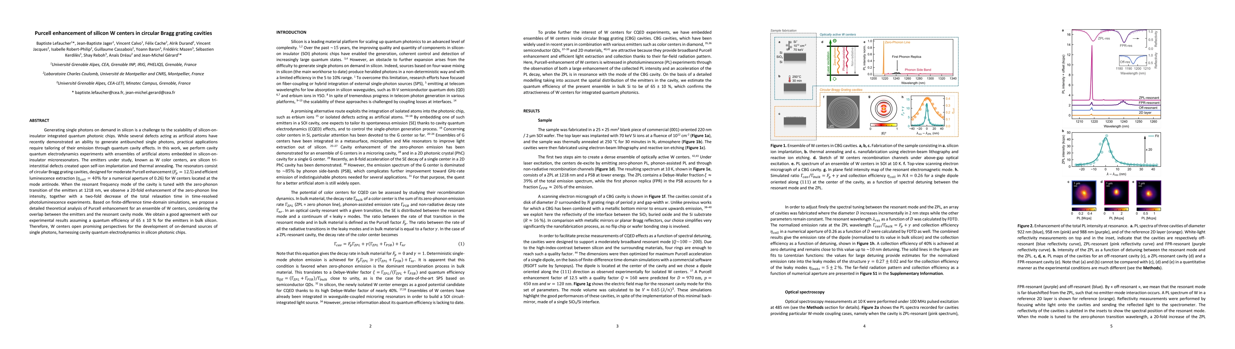
Generating single photons on demand in silicon is a challenge to the scalability of silicon-on-insulator integrated quantum photonic chips. While several defects acting as artificial atoms have rece...

Thumbnail for Investigation of Lasing in Highly Strained Germanium at the Crossover to
  Direct Band Gap

Investigation of Lasing in Highly Strained Germanium at the Crossover to Direct Band Gap

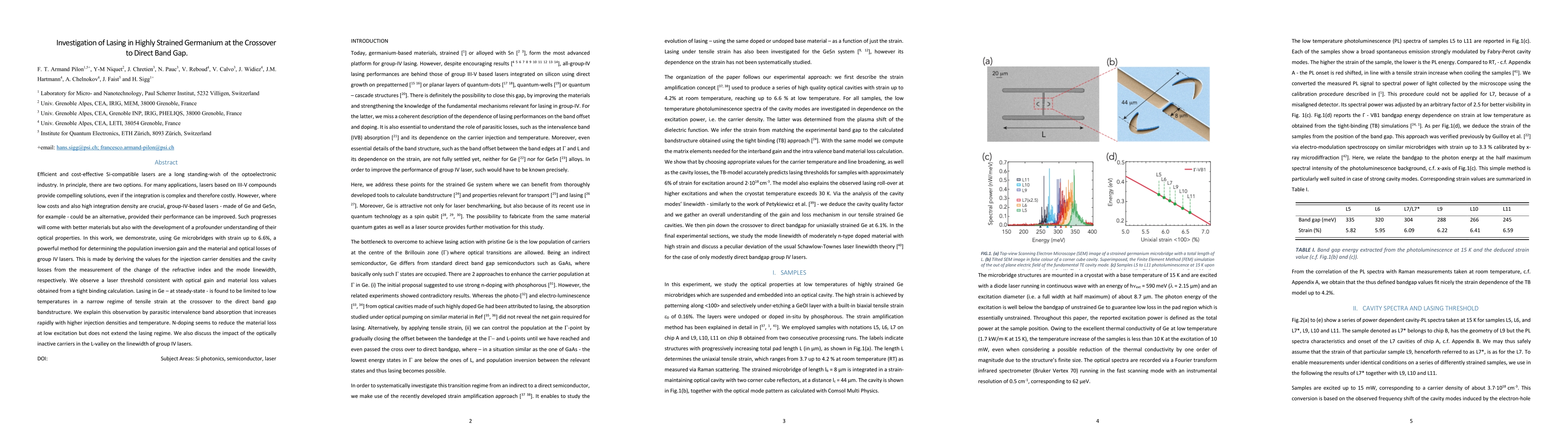
Efficient and cost-effective Si-compatible lasers are a long standing wish of the optoelectronic industry. In principle, there are two options. For many applications, lasers based on III-V compounds...

Thumbnail for Reduced lasing thresholds in GeSn microdisk cavities with defect
  management of the optically active region

Reduced lasing thresholds in GeSn microdisk cavities with defect management of the optically active region

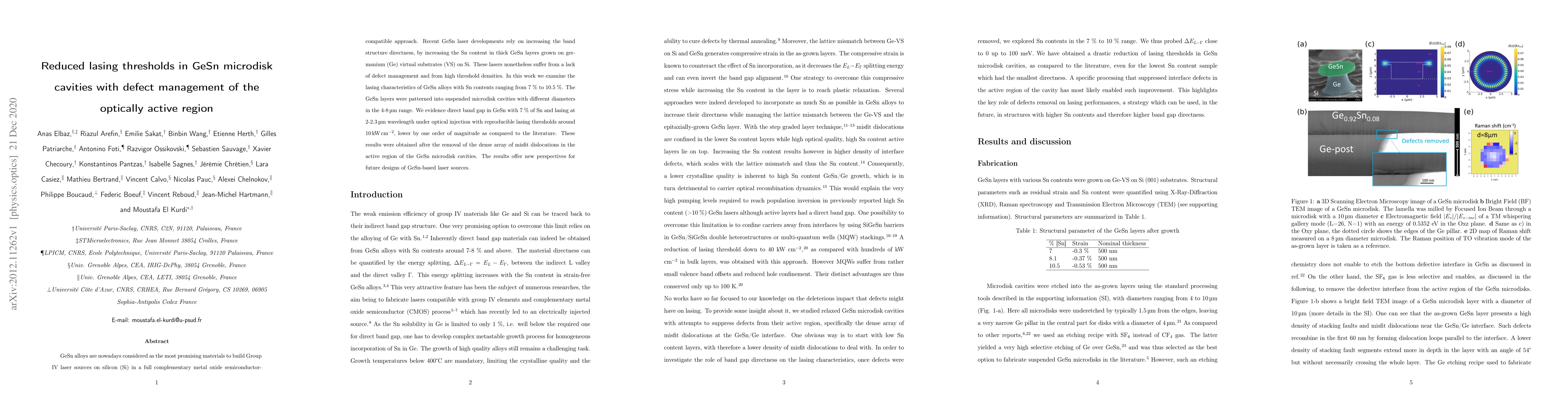
GeSn alloys are nowadays considered as the most promising materials to build Group IV laser sources on silicon (Si) in a full complementary metal oxide semiconductor-compatible approach. Recent GeSn...

Thumbnail for Bright single-photon source in a silicon chip by nanoscale positioning
  of a color center in a microcavity

Bright single-photon source in a silicon chip by nanoscale positioning of a color center in a microcavity

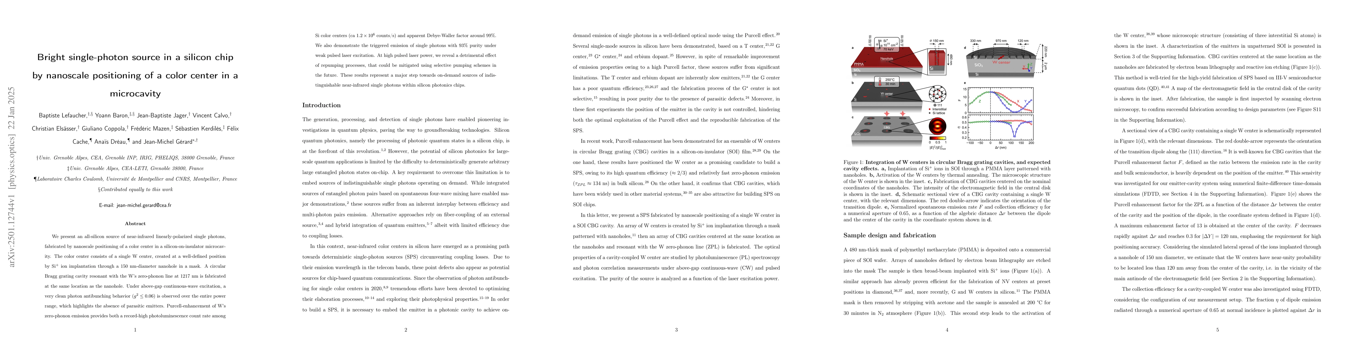
We present an all-silicon source of near-infrared linearly-polarized single photons, fabricated by nanoscale positioning of a color center in a silicon-on-insulator microcavity. The color center consi...

Thumbnail for Growth and Morphology of InN Nanowires on Si<111> and Si<100> at Back-End-Of-Line Compatible Temperatures

Growth and Morphology of InN Nanowires on Si<111> and Si<100> at Back-End-Of-Line Compatible Temperatures

InN nanowires were grown on Si<111> and Si<100> substrates by plasma-assisted molecular beam epitaxy using a thin AlN buffer layer at temperatures compatible with the thermal budget limitation imposed...

This website uses cookies to ensure you get the best experience. Learn more