Statistics
Similar Authors
Papers on arXiv
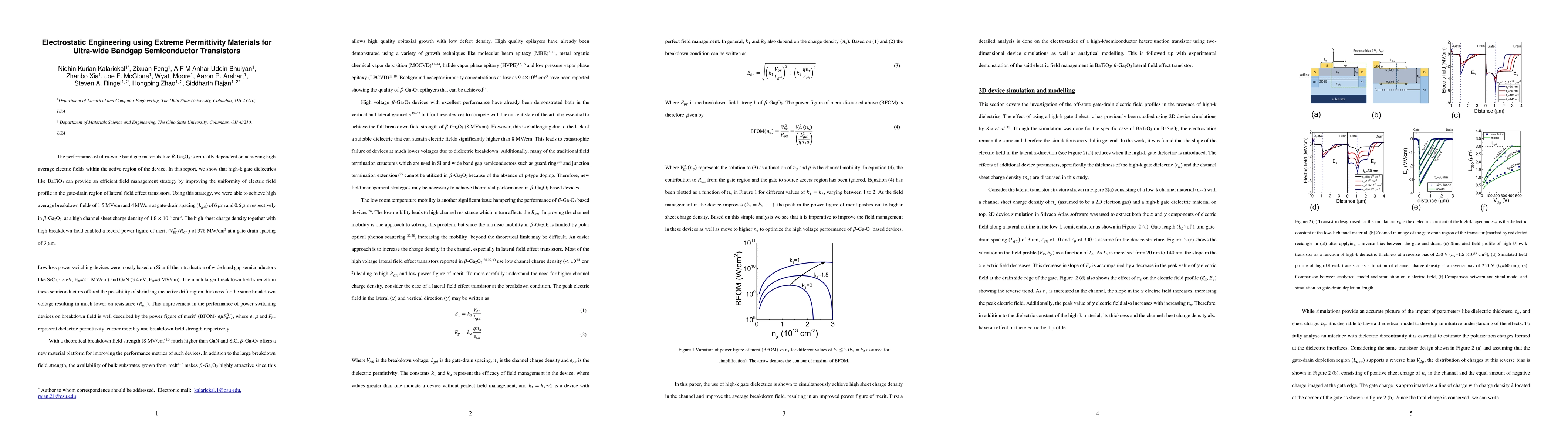
The performance of ultra-wide band gap materials like $\beta$-Ga$_\mathrm{2}$O$_\mathrm{3}$ is critically dependent on achieving high average electric fields within the active region of the device. ...
A new record-high room temperature electron Hall mobility (${\mu}_{RT} = 194\space cm^{2}/V\space s$ at $n\sim 8\times 10^{15}\space cm^{-3}$) for ${\beta}$-Ga2O3 is demonstrated in the unintentiona...
Wide and ultra-wide band gap semiconductors can provide excellent performance due to their high energy band gap, which leads to breakdown electric fields that are more than an order of magnitude hig...
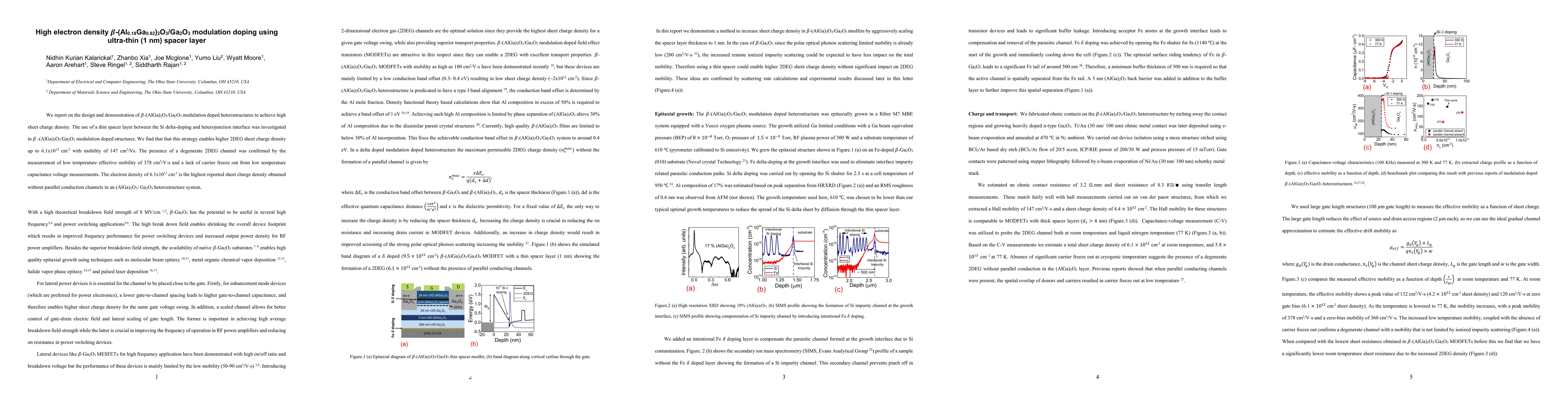
We report on the design and demonstration of ${\beta}-(Al_{0.18}Ga_{0.82})_2O_3/Ga_2O_3$ modulation doped heterostructures to achieve high sheet charge density. The use of a thin spacer layer betwee...
We report on the origin of high Si flux observed during the use of Si as a doping source in plasma assisted MBE growth of \b{eta}-Ga2O3. We show on the basis of secondary ion mass spectroscopy (SIMS...