Academic Profile
Statistics
Similar Authors
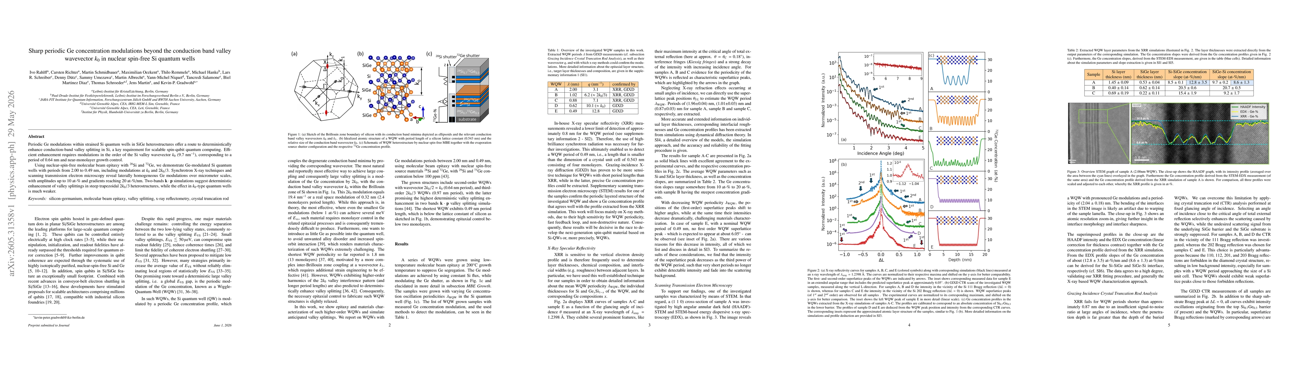
Papers on arXiv
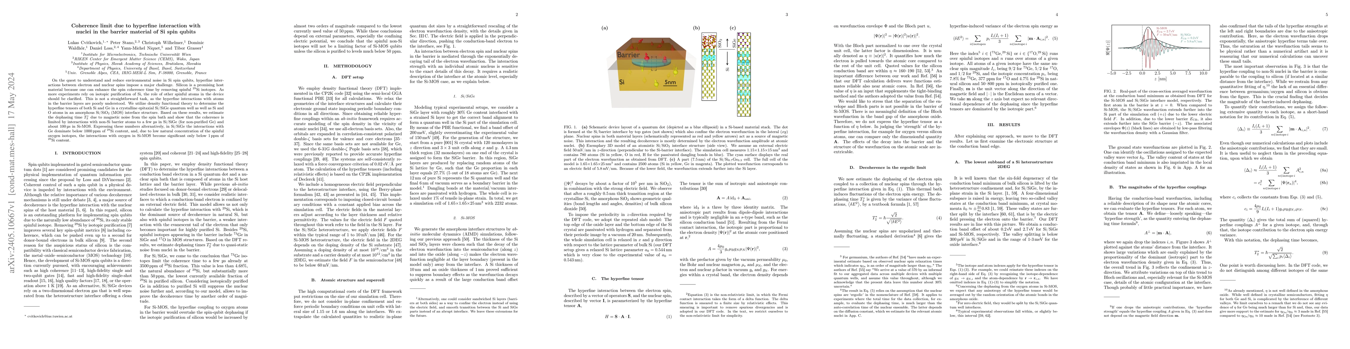
On the quest to understand and reduce environmental noise in Si spin qubits, hyperfine interactions between electron and nuclear spins impose a major challenge. Silicon is a promising host material ...
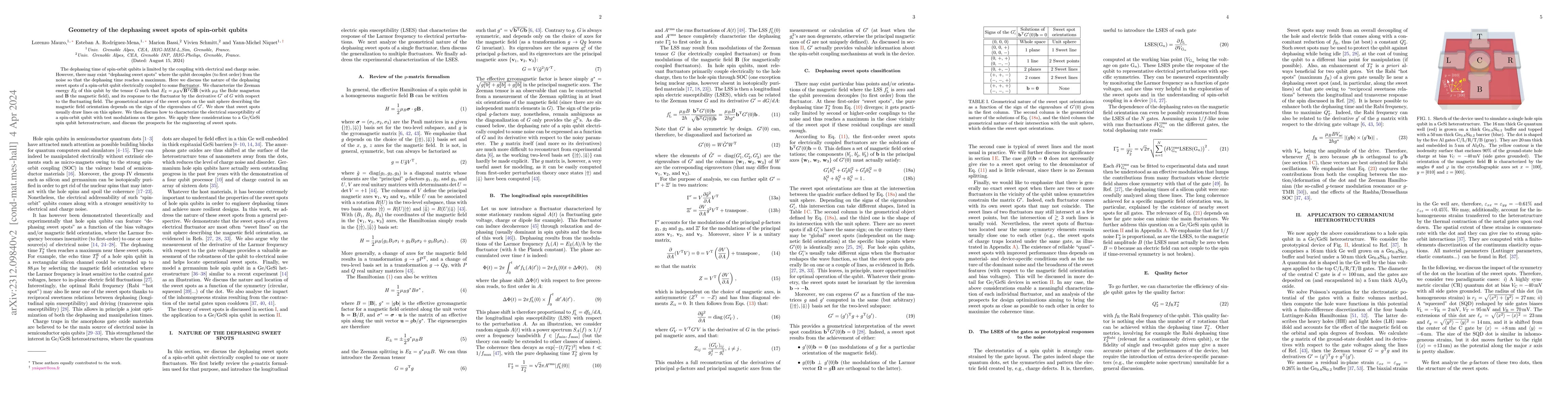
The dephasing time of spin-orbit qubits is limited by the coupling with electrical and charge noise. However, there may exist "dephasing sweet spots" where the qubit decouples (to first order) from ...
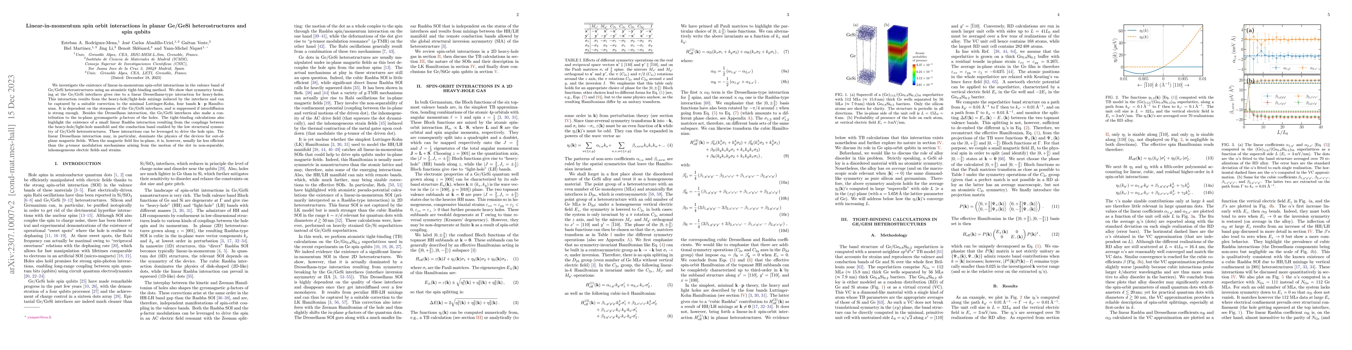
We investigate the existence of linear-in-momentum spin-orbit interactions in the valence band of Ge/GeSi heterostructures using an atomistic tight-binding method. We show that symmetry breaking at ...
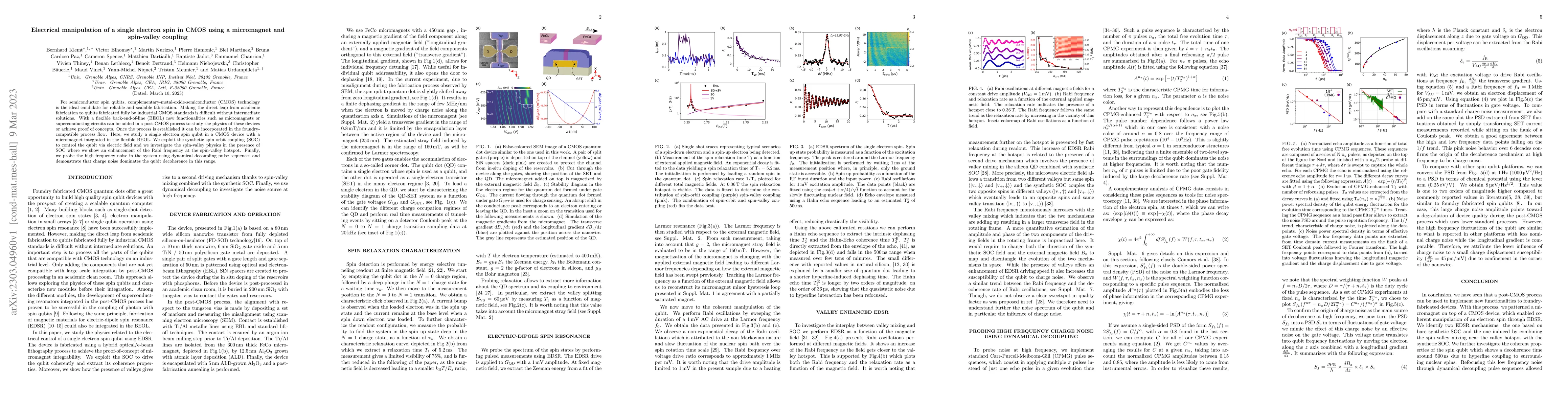
For semiconductor spin qubits, complementary-metal-oxide-semiconductor (CMOS) technology is the ideal candidate for reliable and scalable fabrication. Making the direct leap from academic fabricatio...
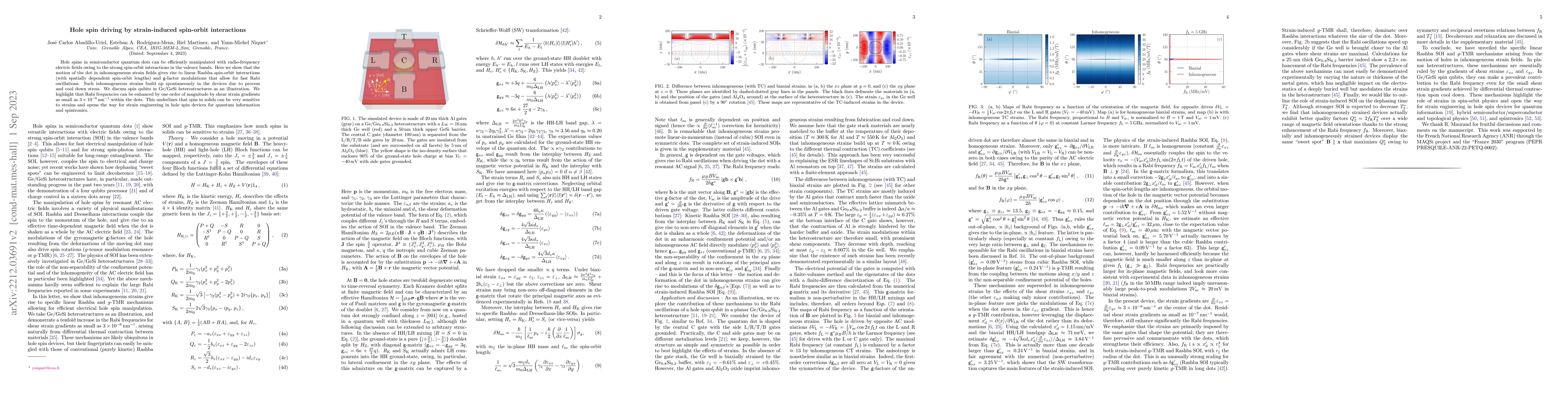
Hole spins in semiconductor quantum dots can be efficiently manipulated with radio-frequency electric fields owing to the strong spin-orbit interactions in the valence bands. Here we show that the m...
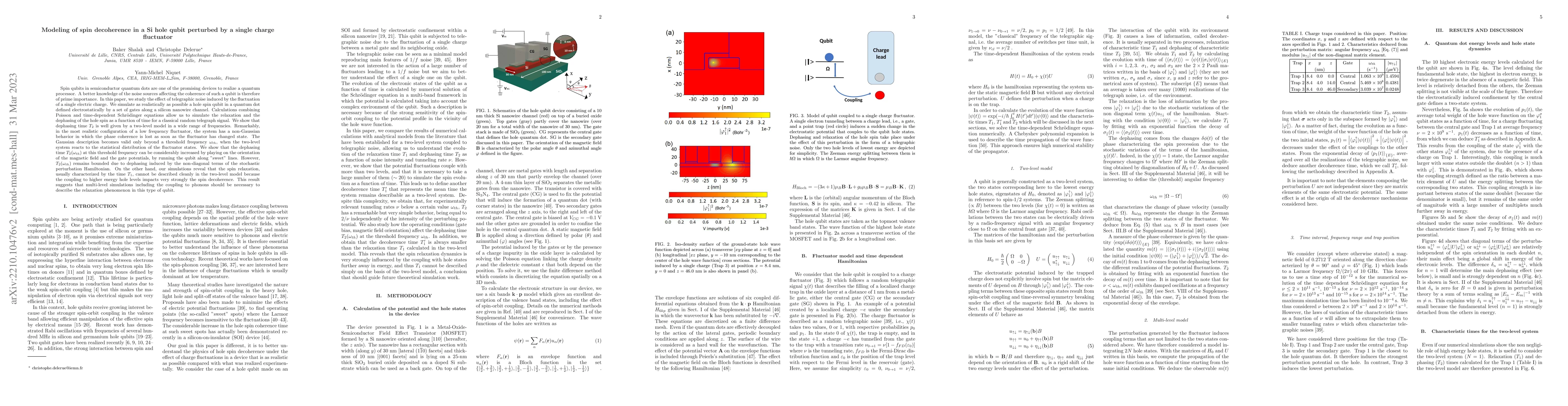
Spin qubits in semiconductor quantum dots are one of the promizing devices to realize a quantum processor. A better knowledge of the noise sources affecting the coherence of such a qubit is therefor...
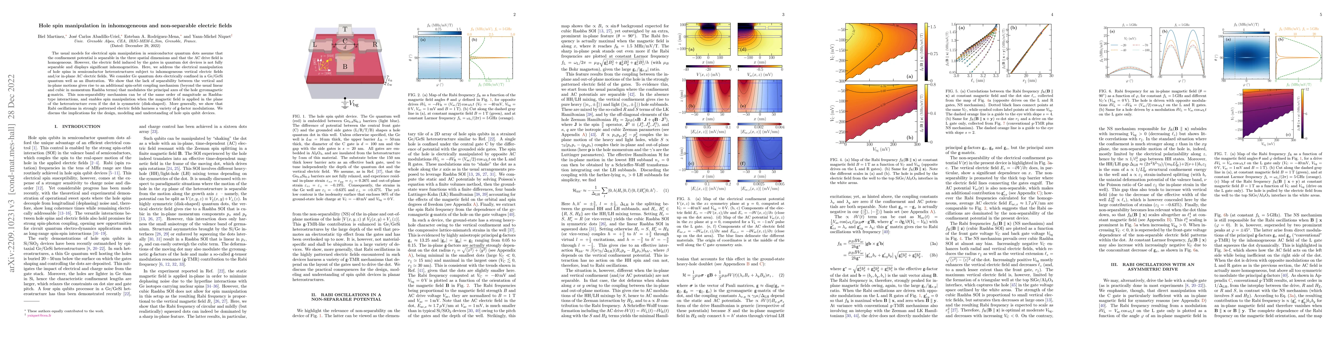
The usual models for electrical spin manipulation in semiconductor quantum dots assume that the confinement potential is separable in the three spatial dimensions and that the AC drive field is homo...
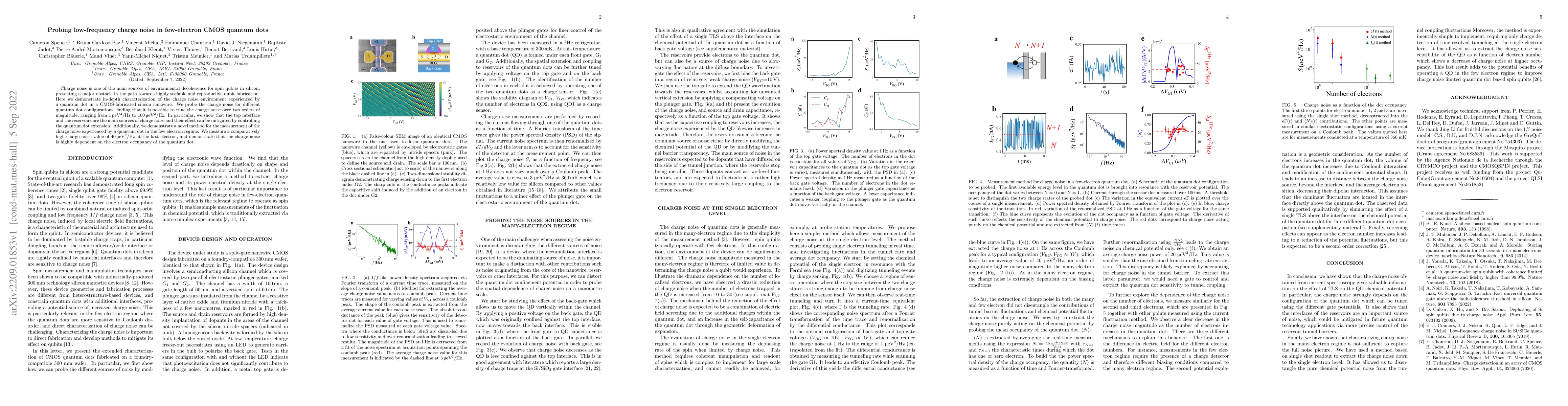
Charge noise is one of the main sources of environmental decoherence for spin qubits in silicon, presenting a major obstacle in the path towards highly scalable and reproducible qubit fabrication. ...
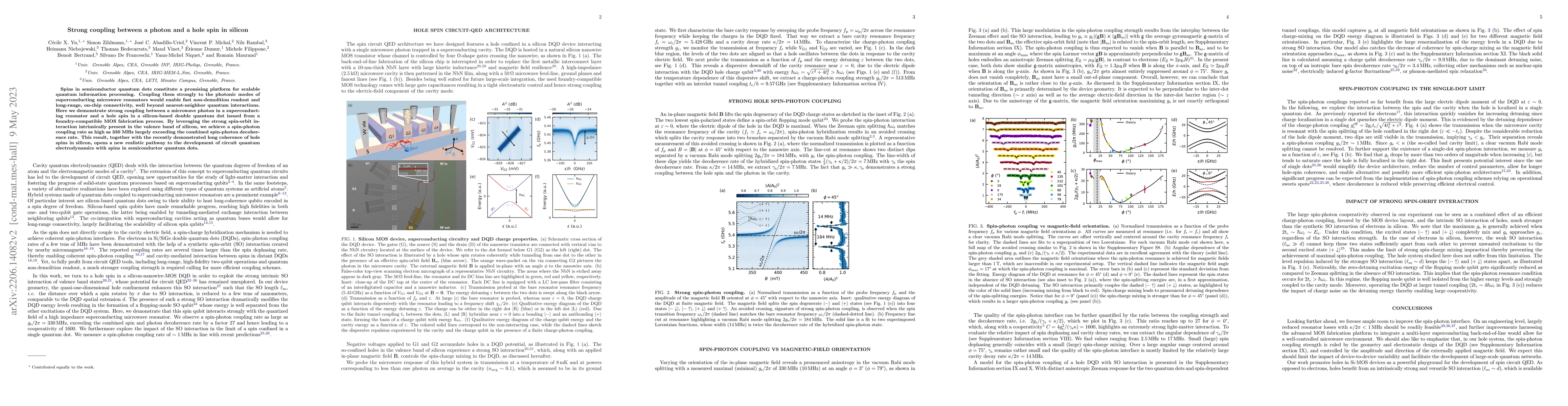
Spins in semiconductor quantum dots constitute a promising platform for scalable quantum information processing. Coupling them strongly to the photonic modes of superconducting microwave resonators ...
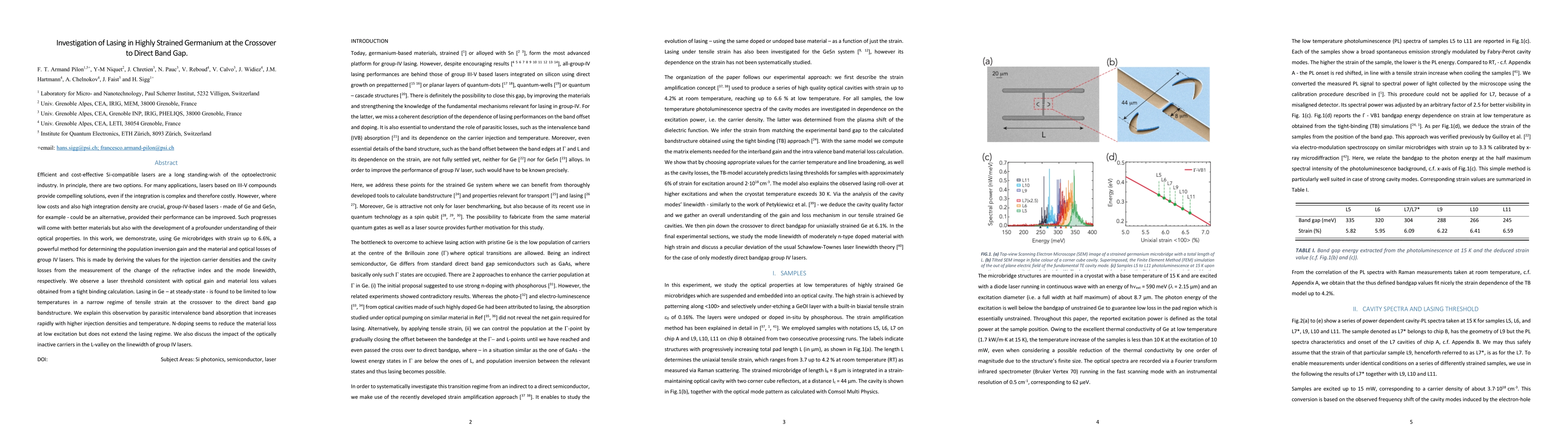
Efficient and cost-effective Si-compatible lasers are a long standing wish of the optoelectronic industry. In principle, there are two options. For many applications, lasers based on III-V compounds...
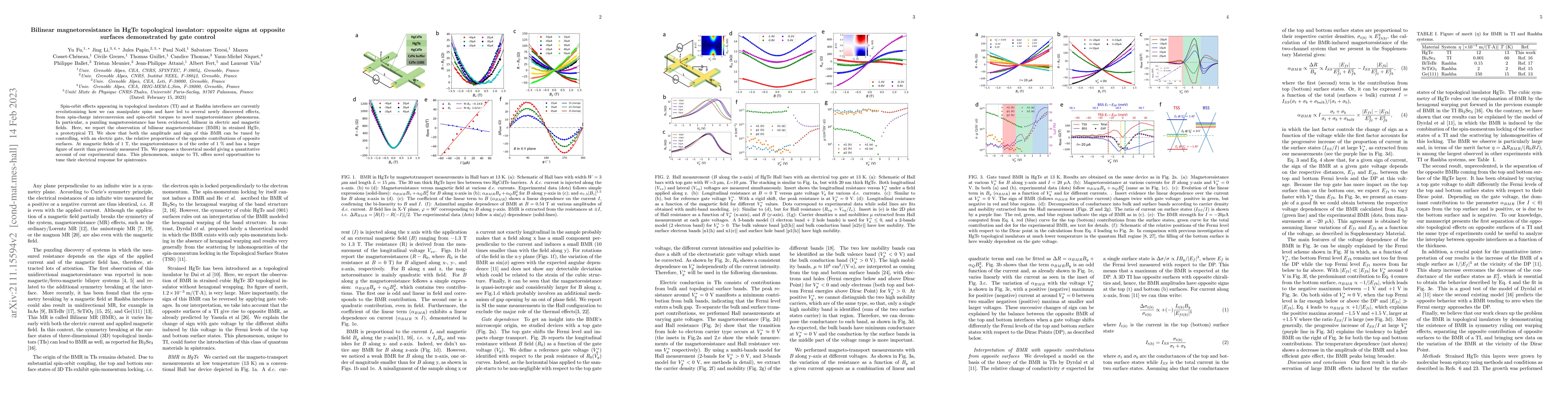
Spin-orbit effects appearing in topological insulators (TI) and at Rashba interfaces are currently revolutionizing how we can manipulate spins and have led to several newly discovered effects, from ...
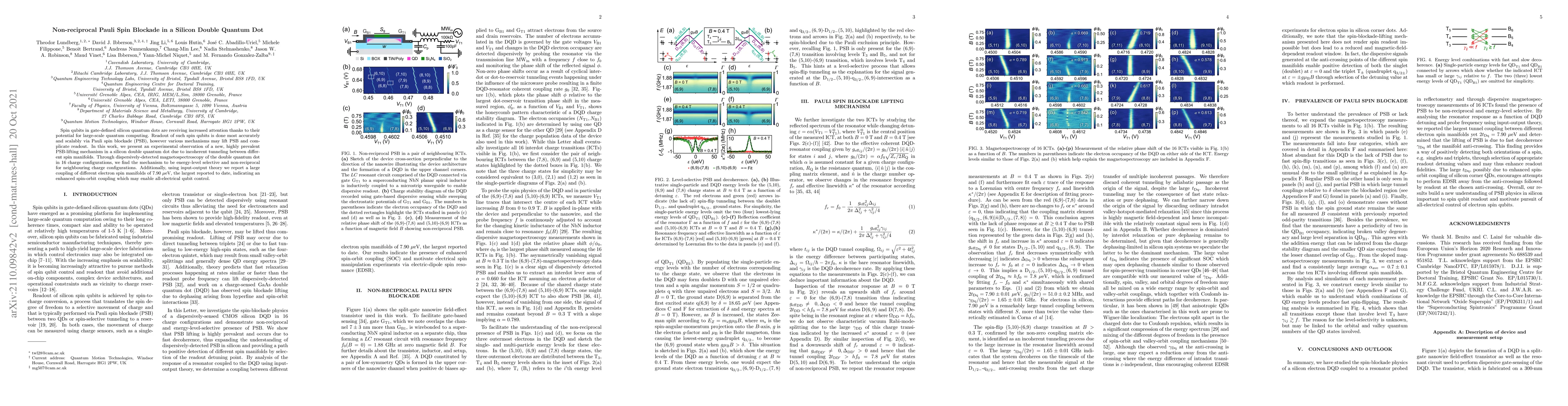
Spin qubits in gate-defined silicon quantum dots are receiving increased attention thanks to their potential for large-scale quantum computing. Readout of such spin qubits is done most accurately an...
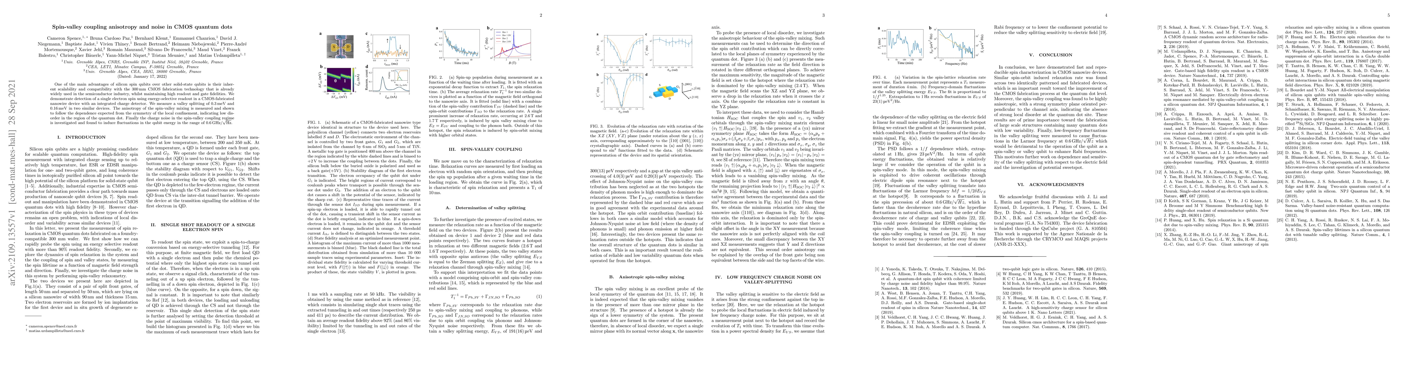
One of the main advantages of silicon spin qubits over other solid-state qubits is their inherent scalability and compatibility with the 300 mm CMOS fabrication technology that is already widely use...
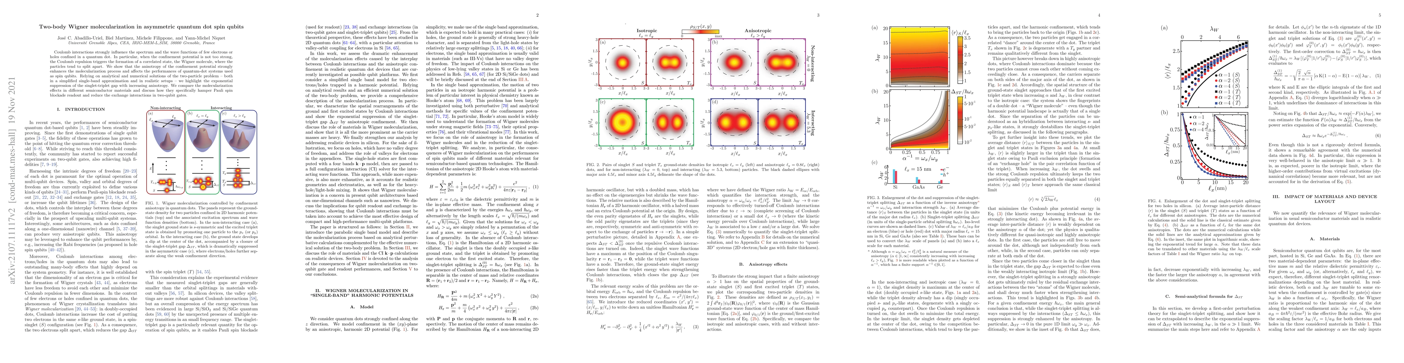
Coulomb interactions strongly influence the spectrum and the wave functions of few electrons or holes confined in a quantum dot. In particular, when the confinement potential is not too strong, the ...
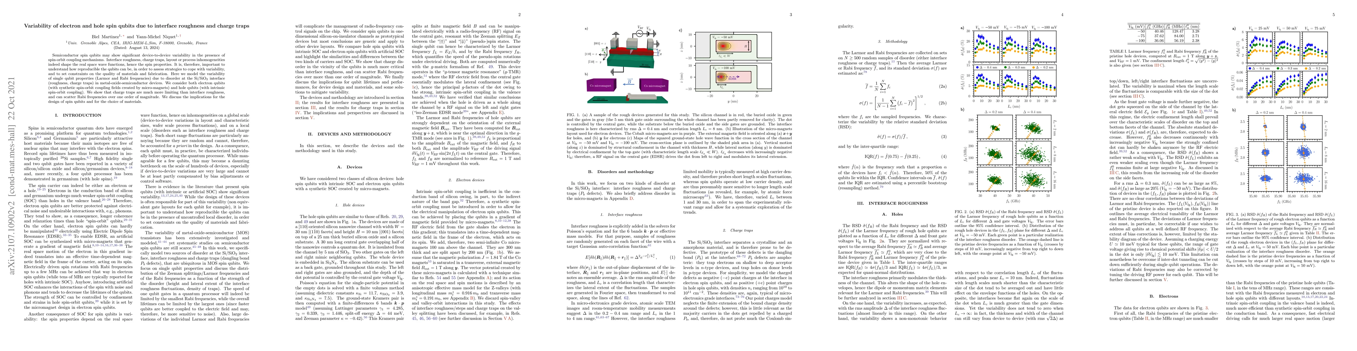
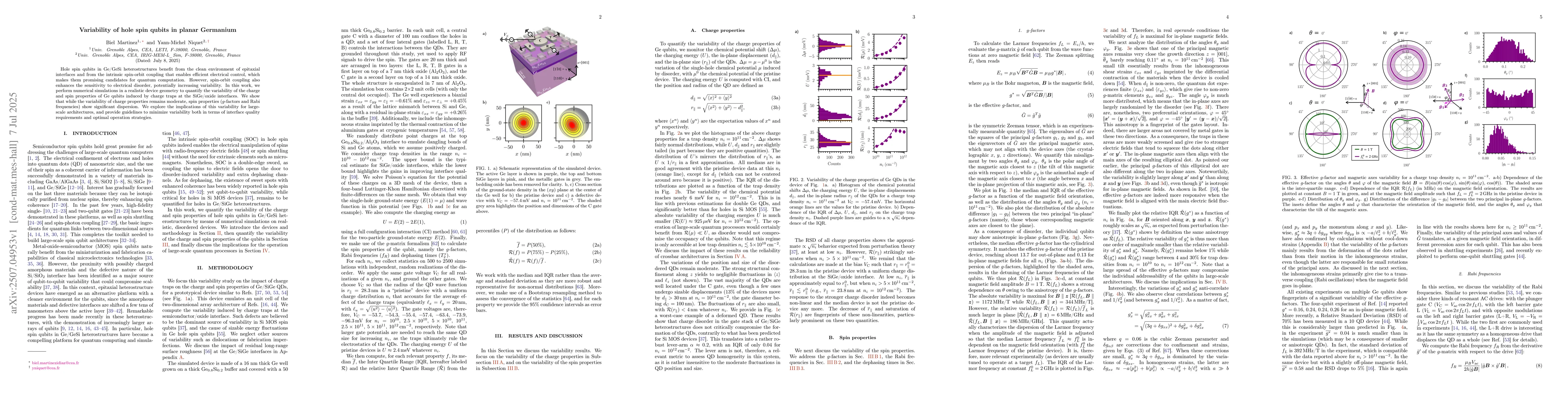
Semiconductor spin qubits may show significant device-to-device variability in the presence of spin-orbit coupling mechanisms. Interface roughness, charge traps, layout or process inhomogeneities in...
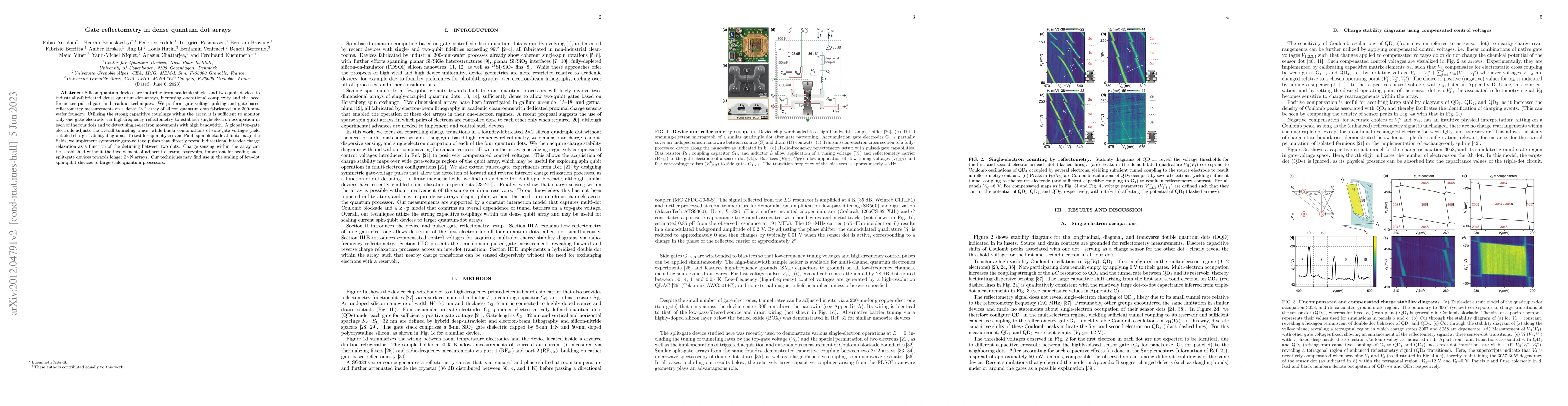
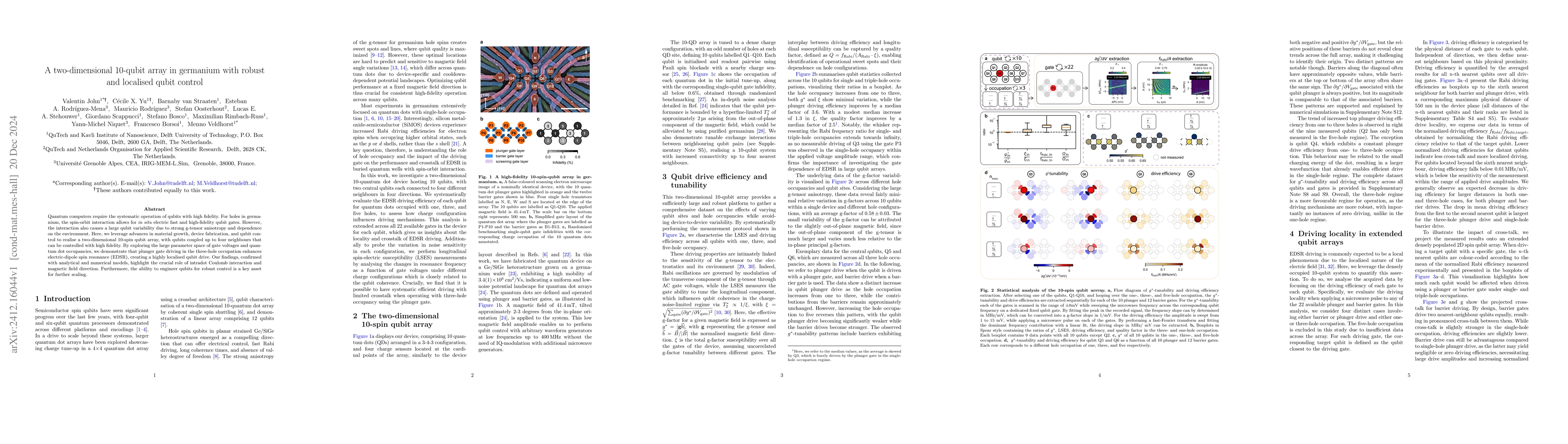
Silicon quantum devices are maturing from academic single- and two-qubit devices to industrially-fabricated dense quantum-dot (QD) arrays, increasing operational complexity and the need for better p...
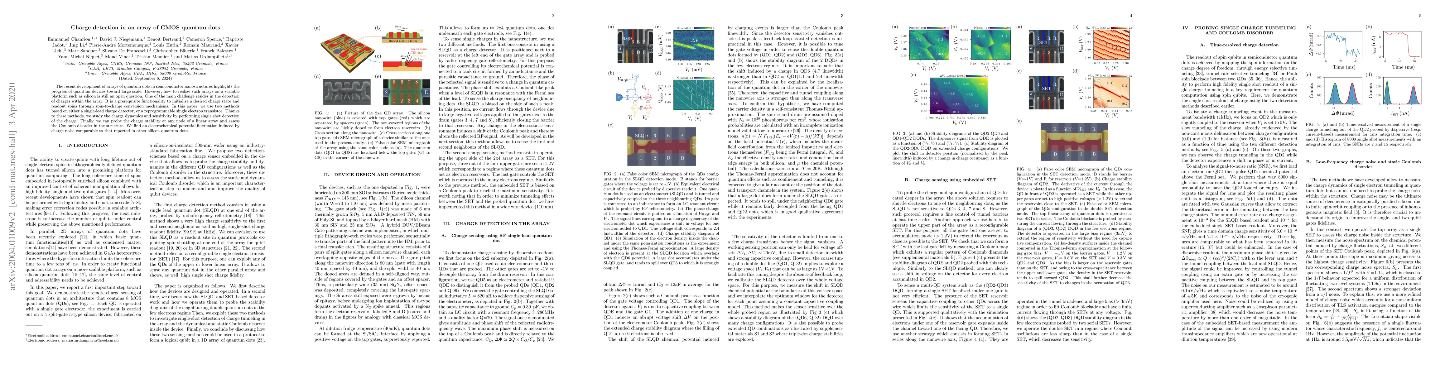
The recent development of arrays of quantum dots in semiconductor nanostructures highlights the progress of quantum devices toward large scale. However, how to realize such arrays on a scalable plat...
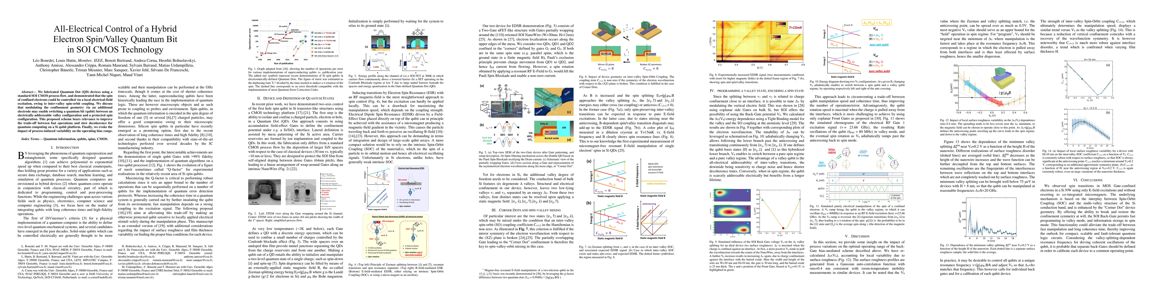
We fabricated Quantum Dot (QD) devices using a standard SOI CMOS process flow, and demonstrated that the spin of confined electrons could be controlled via a local electrical-field excitation, owing...
Spins in gate-defined silicon quantum dots are promising candidates for implementing large-scale quantum computing. To read the spin state of these qubits, the mechanism that has provided the highes...
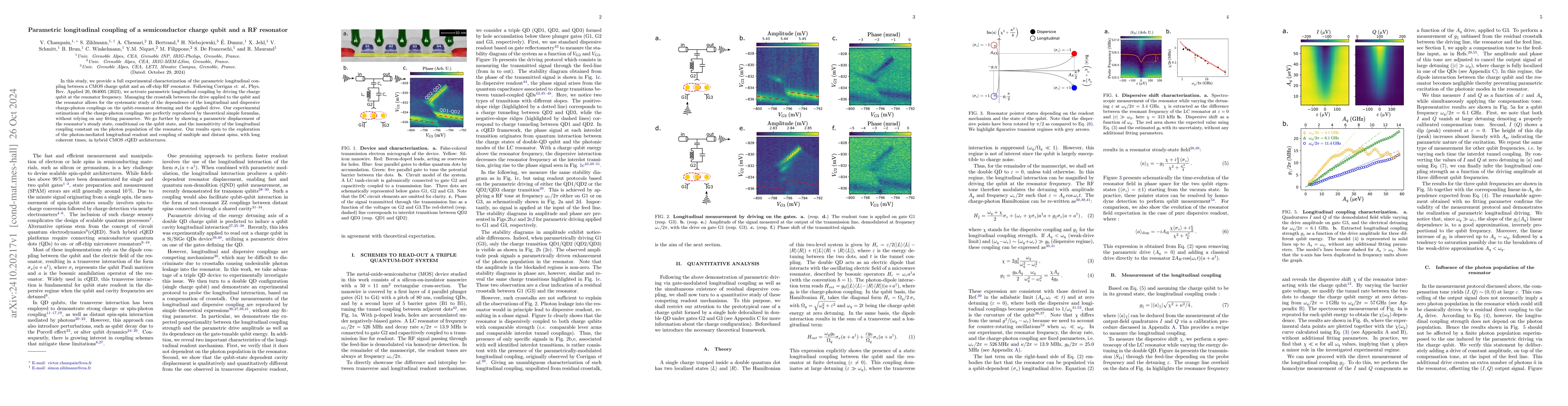
In this study, we provide a full experimental characterization of the parametric longitudinal coupling between a CMOS charge qubit and an off-chip RF resonator. Following Corrigan et al, Phys. Rev. Ap...
This article introduces a groundbreaking analytical workflow designed for the holistic characterisation, modelling and physical simulation of device heterostructures. Our innovative workflow autonomou...
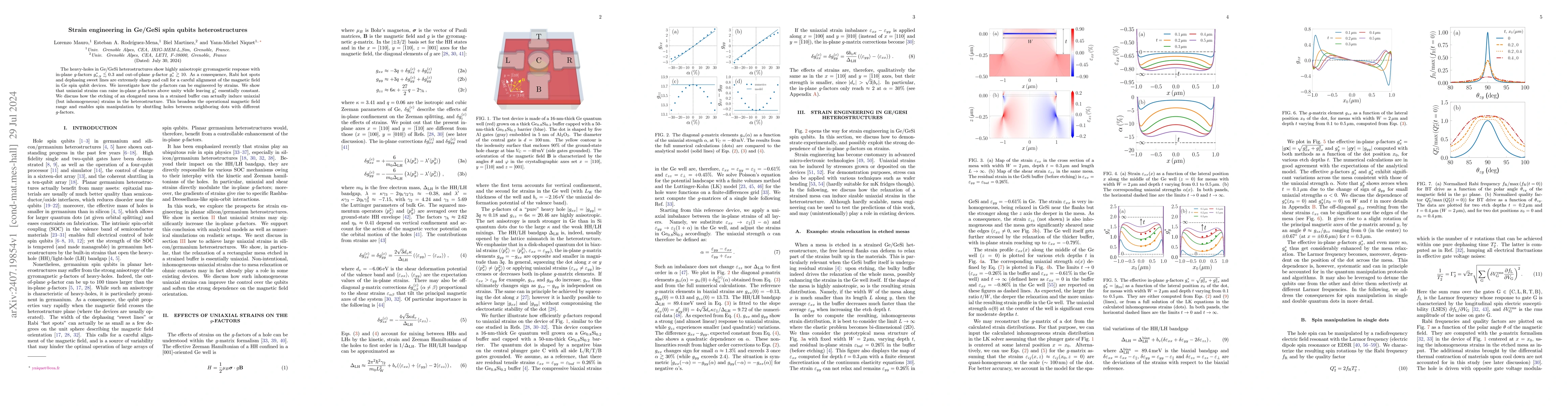
The heavy-holes in Ge/GeSi heterostructures show highly anisotropic gyromagnetic response with in-plane $g$-factors $g_{x,y}^*\lesssim 0.3$ and out-of-plane $g$-factor $g_z^*\gtrsim 10$. As a conseque...
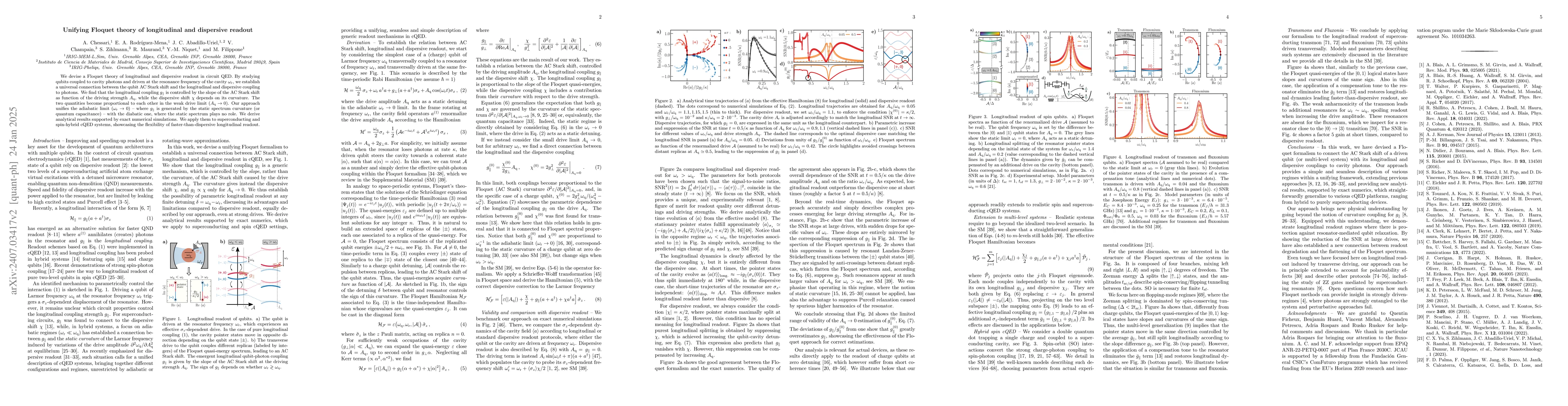
We devise a Floquet theory of longitudinal and dispersive readout in circuit QED. By studying qubits coupled to cavity photons and driven at the resonance frequency of the cavity $\omega_{\rm r}$, we ...
Quantum computers require the systematic operation of qubits with high fidelity. For holes in germanium, the spin-orbit interaction allows for \textit{in situ} electric fast and high-fidelity qubit ga...
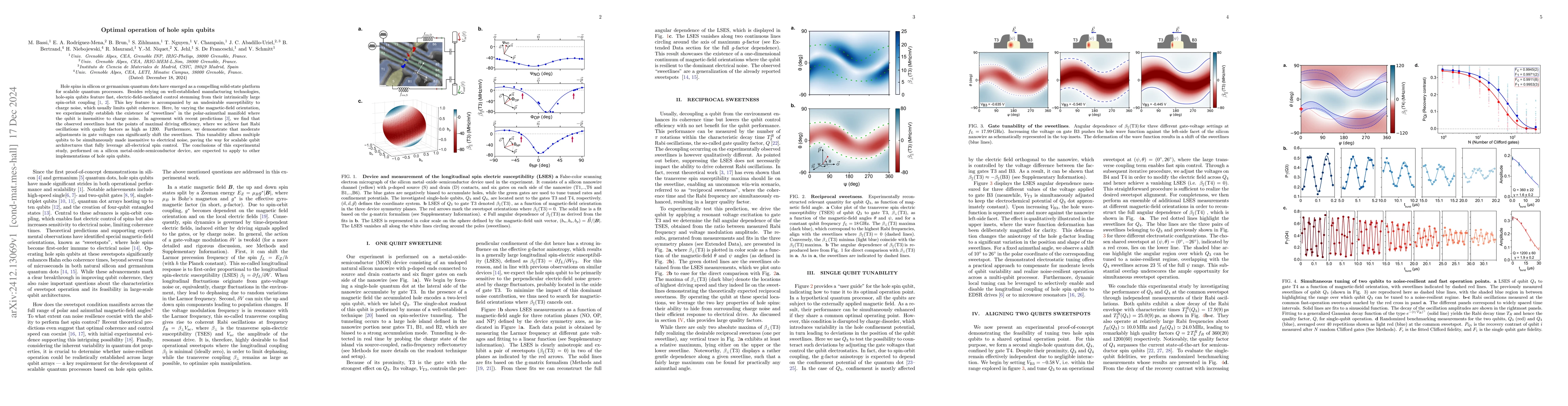
Hole spins in silicon or germanium quantum dots have emerged as a compelling solid-state platform for scalable quantum processors. Besides relying on well-established manufacturing technologies, hole-...
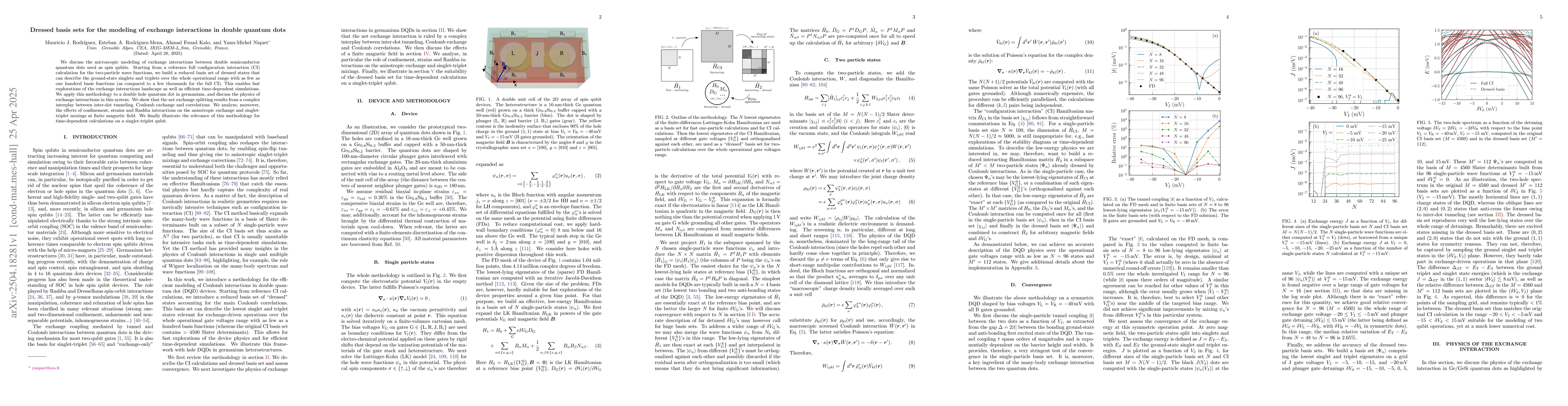
We discuss the microscopic modeling of exchange interactions between double semiconductor quantum dots used as spin qubits. Starting from a reference full configuration interaction (CI) calculation fo...
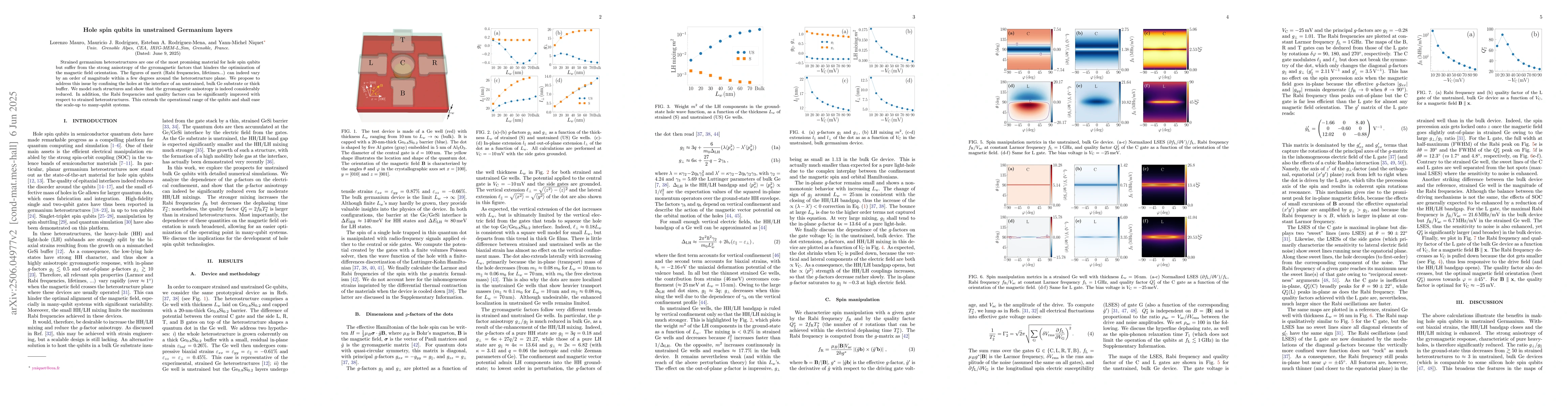
Strained germanium heterostructures are one of the most promising material for hole spin qubits but suffer from the strong anisotropy of the gyromagnetic factors that hinders the optimization of the m...
Hole spin qubits in Ge/GeSi heterostructures benefit from the clean environment of epitaxial interfaces and from the intrinsic spin-orbit coupling that enables efficient electrical control, which make...
Recent advances in the scaling of spin qubits have led to the development of sparse architectures where spin qubits are distributed across multiple quantum dots. This distributed approach enables qubi...
We discuss the choice and implementation of inter-valley potentials in the so-called two bands k.p model for the opposite X, Y or Z valleys of silicon. We focus on the description of valley splittings...
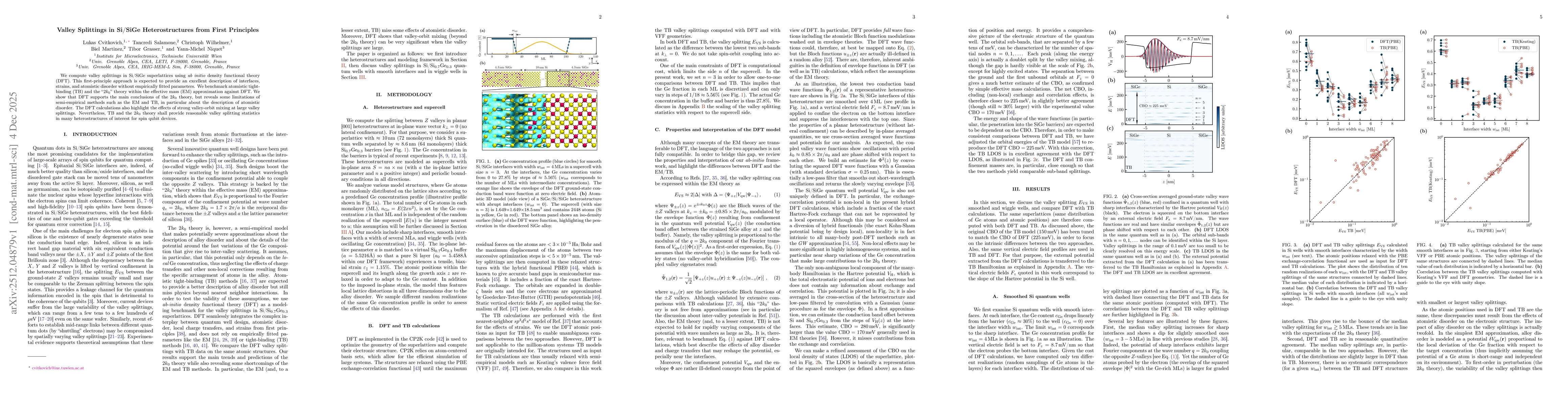
We compute valley splittings in Si/SiGe superlattices using ab initio density functional theory (DFT). This first-principle approach is expected to provide an excellent description of interfaces, stra...
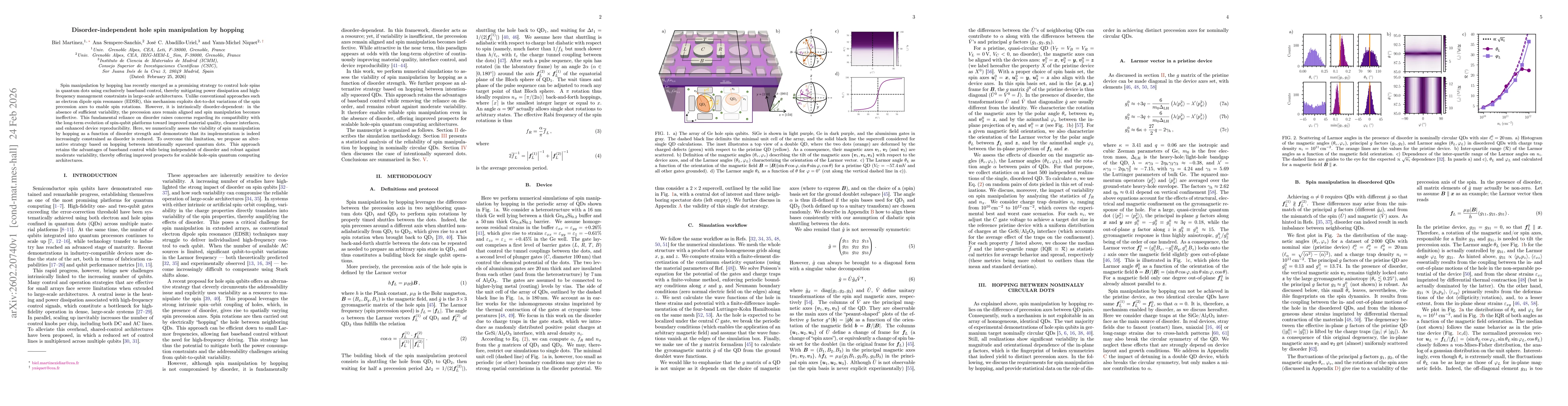
Spin manipulation by hopping has recently emerged as a promising strategy to control hole spins in quantum dots using exclusively baseband control, thereby mitigating power dissipation and high-freque...
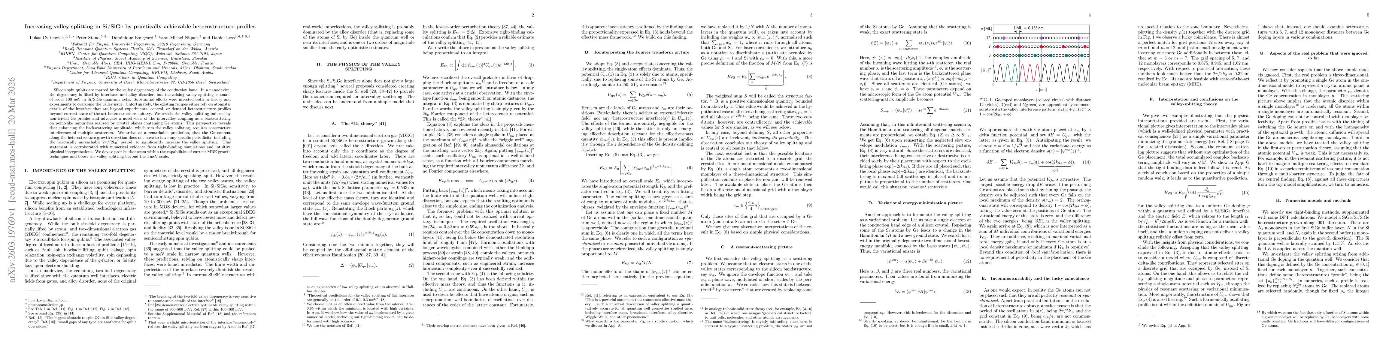
Silicon spin qubits are marred by the valley degeneracy of the conduction band. In a nanodevice, the degeneracy is lifted by interfaces and alloy disorder, but the arising valley splitting is small, o...
Periodic Ge modulations within strained Si quantum wells in SiGe heterostructures offer a route to deterministically enhance conduction-band valley splitting in Si, a key requirement for scalable spin...