Academic Profile
Statistics
Similar Authors
Papers on arXiv
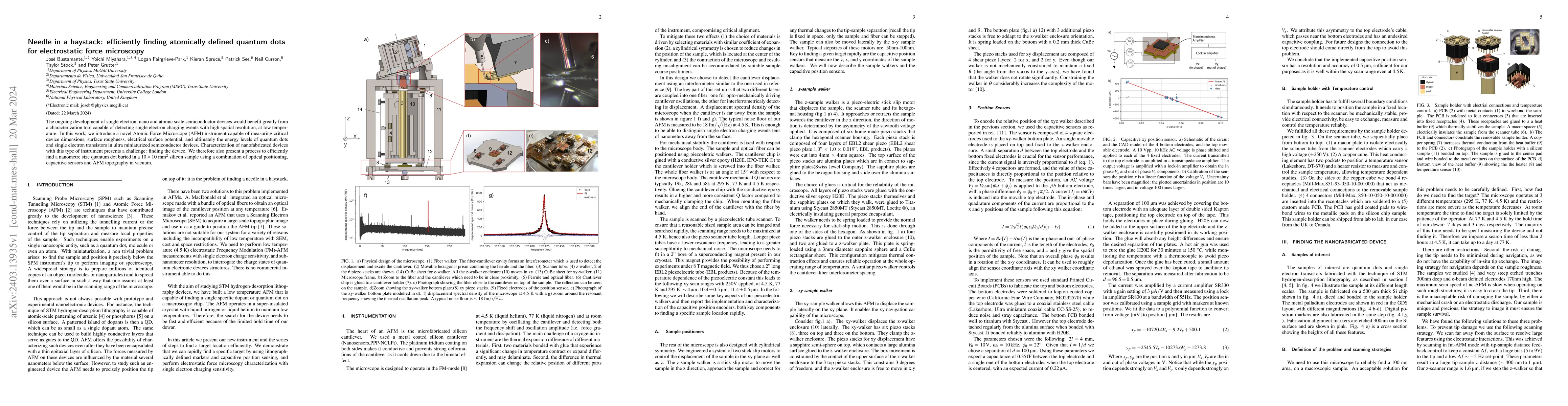
The ongoing development of single electron, nano and atomic scale semiconductor devices would benefit greatly from a characterization tool capable of detecting single electron charging events with h...
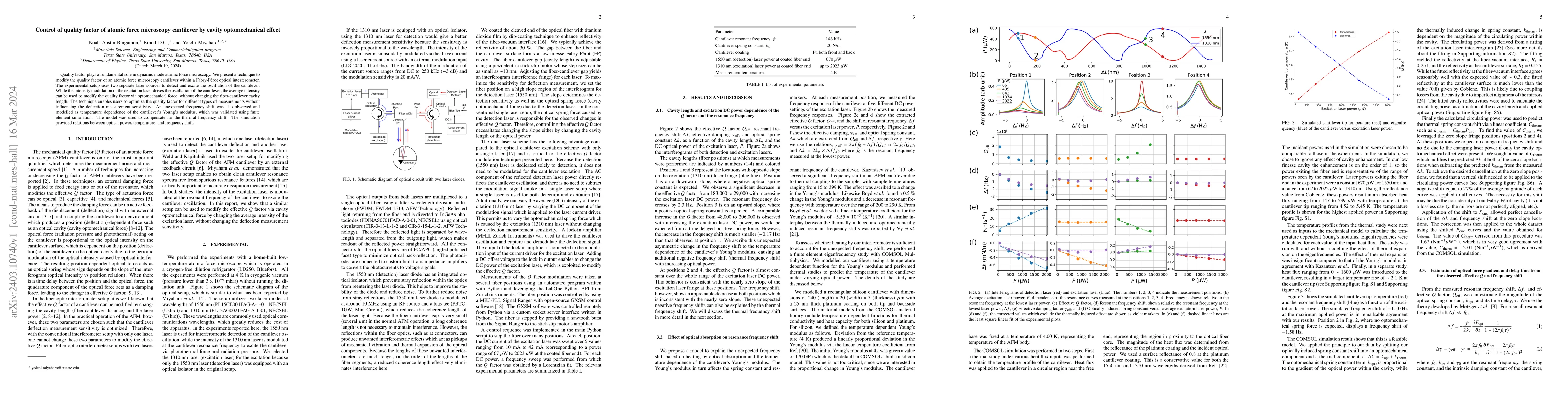
Quality factor plays a fundamental role in dynamic mode atomic force microscopy. We present a technique to modify the quality factor of an atomic force microscopy cantilever within a Fabry-P\'erot o...
Moir\'e superlattices formed by vertically stacking van der Waals layers host a rich variety of correlated electronic phases and function as novel photonic materials. The moir\'e potential of the su...
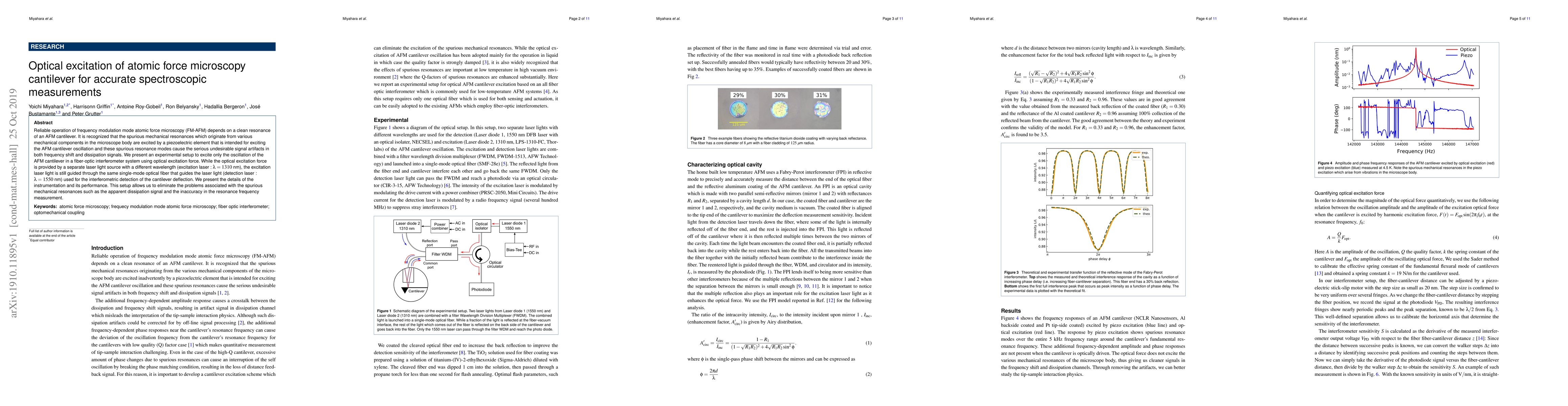
Reliable operation of frequency modulation mode atomic force microscopy (FM-AFM) depends on a clean resonance of an AFM cantilever. It is recognized that the spurious mechanical resonances which ori...
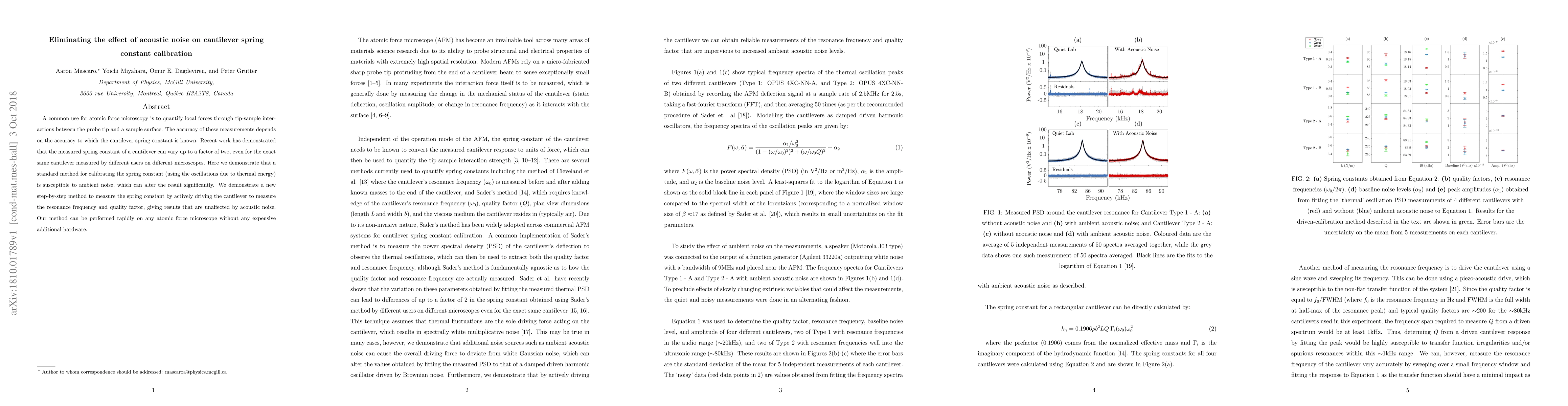
A common use for atomic force microscopy is to quantify local forces through tip-sample interactions between the probe tip and a sample surface. The accuracy of these measurements depends on the acc...
Actin and myosin drive many instances of force generation, deformation, and shape change in cells, tissues, and organisms. In particular, cytoskeletal actomyosin is remarkable in its adaptive architec...
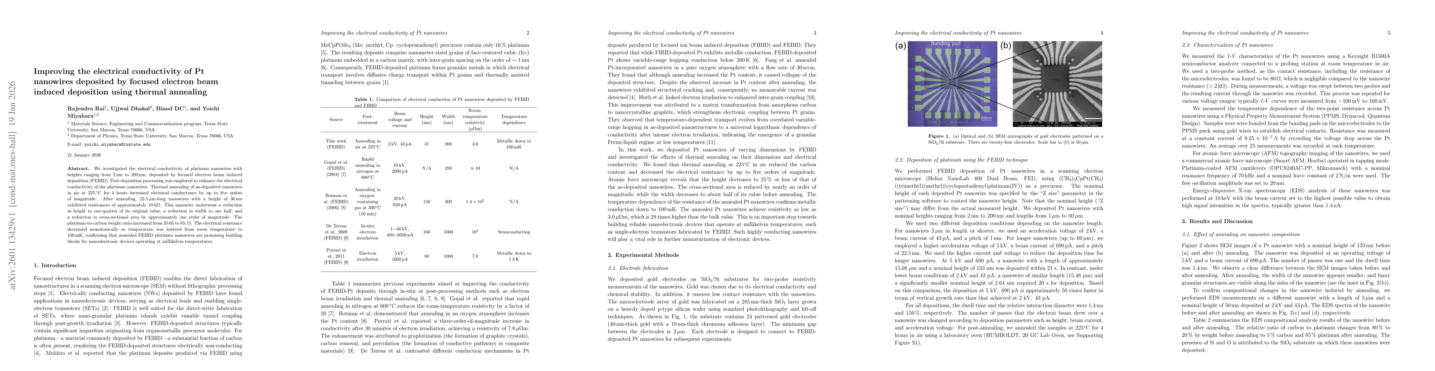
We investigated the electrical conductivity of platinum nanowires with heights ranging from 2 nm to 200 nm, deposited by focused electron beam induced deposition (FEBID). Post-deposition processing wa...