ArxivLens
Z
Researcher

Zhaoli Gao

5 papers on arXiv

5 arXiv Papers
10 Total Publications
Profile

Academic Profile

Name Zhaoli Gao
Total Papers 10
Scholar Profile View on Semantic Scholar
Metrics

Statistics

5 arXiv Papers
10 Total Publications
Publications

Papers on arXiv

Thumbnail for Emergent Moir\'e fringes in direct-grown quasicrystal
arXiv
Emergent Moir\'e fringes in direct-grown quasicrystal

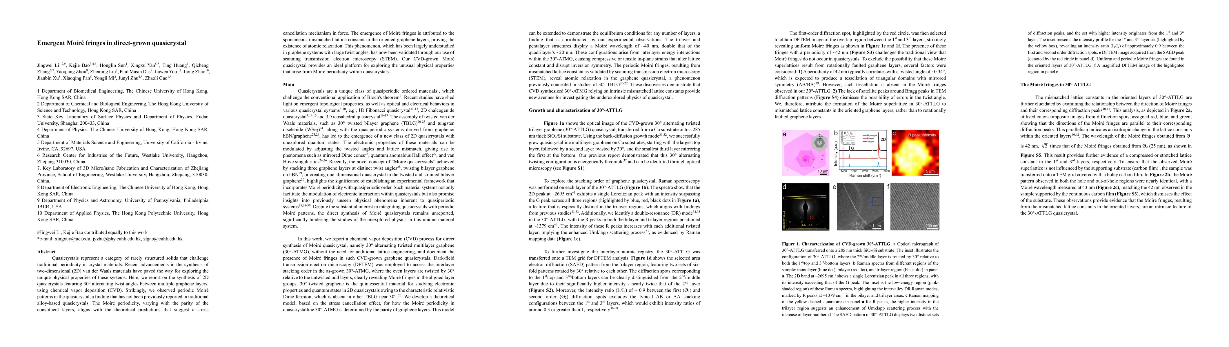
Quasicrystals represent a category of rarely structured solids that challenge traditional periodicity in crystal materials. Recent advancements in the synthesis of two-dimensional (2D) van der Waals...

Thumbnail for Electrically Tunable Magnetoconductance of Close-Packed CVD Bilayer
  Graphene Layer Stacking Walls
arXiv
Electrically Tunable Magnetoconductance of Close-Packed CVD Bilayer Graphene Layer Stacking Walls

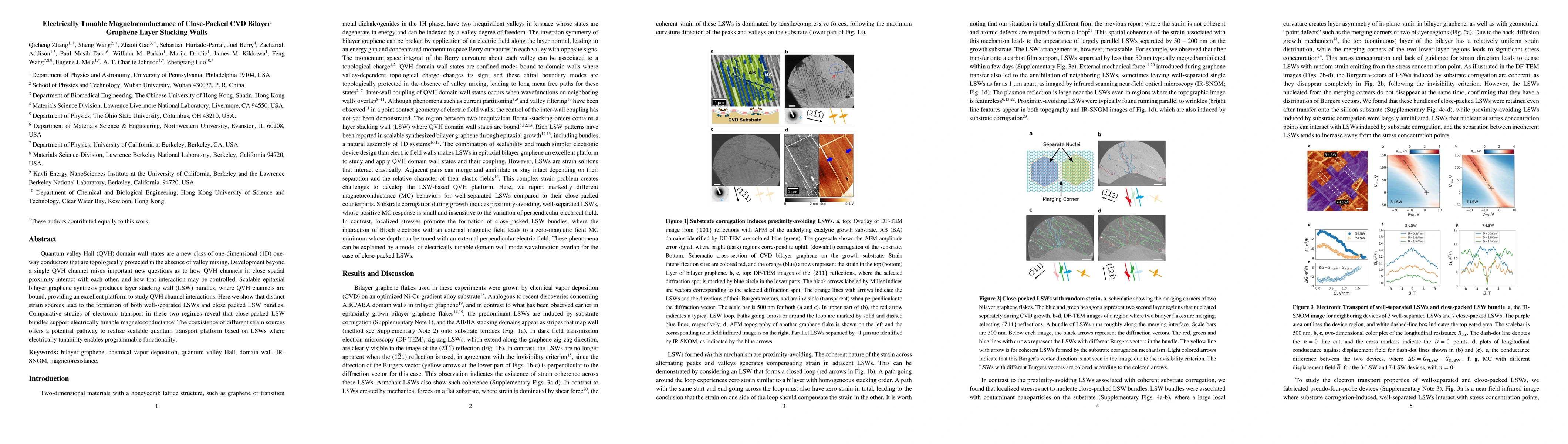
Quantum valley Hall (QVH) domain wall states are a new class of one-dimensional (1D) one-way conductors that are topologically protected in the absence of valley mixing. Development beyond a single ...

Thumbnail for Transmission-matrix Quantitative Phase Profilometry for Accurate and
  Fast Thickness Mapping of 2D Materials
arXiv
Transmission-matrix Quantitative Phase Profilometry for Accurate and Fast Thickness Mapping of 2D Materials

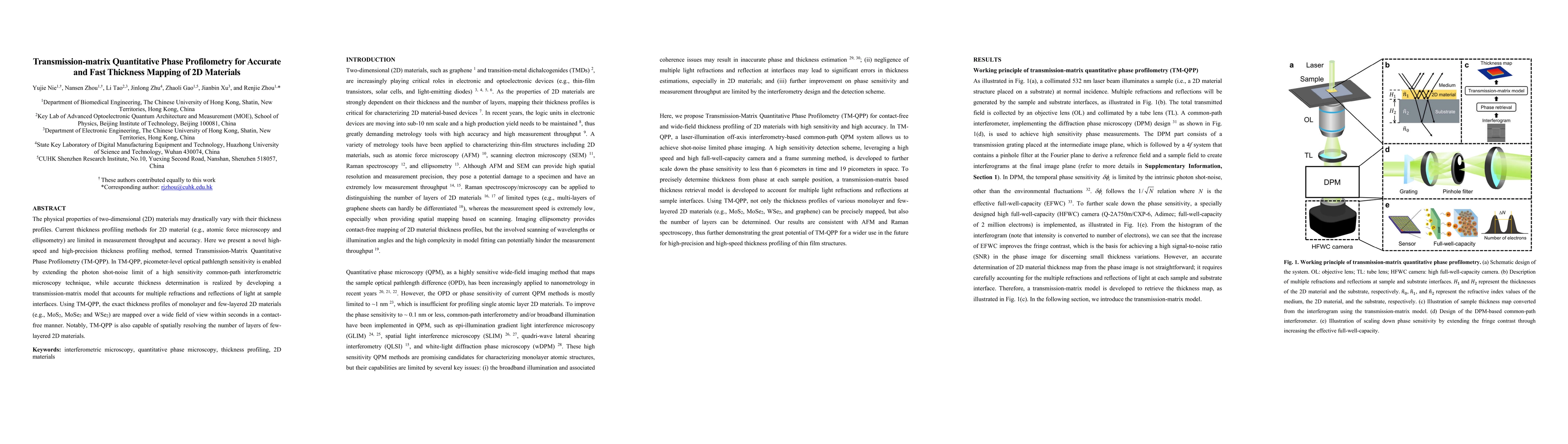
The physical properties of two-dimensional (2D) materials may drastically vary with their thickness profiles. Current thickness profiling methods for 2D material (e.g., atomic force microscopy and e...

Thumbnail for Controlled Growth of Large-Area Bilayer Tungsten Diselenides with
  Lateral P-N Junctions
arXiv
Controlled Growth of Large-Area Bilayer Tungsten Diselenides with Lateral P-N Junctions

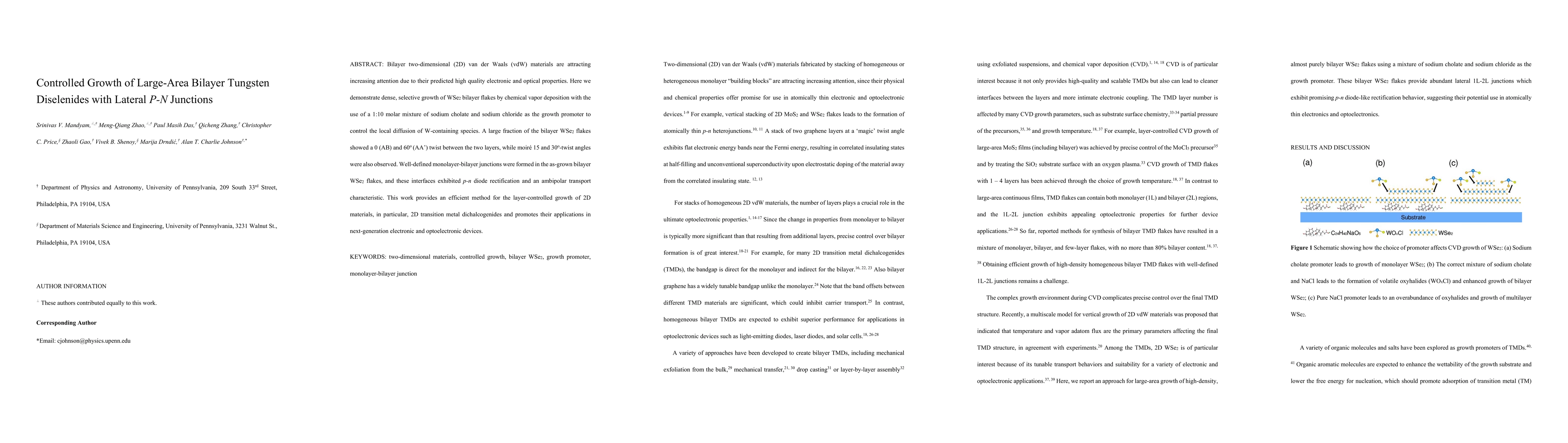
Bilayer two-dimensional (2D) van der Waals (vdW) materials are attracting increasing attention due to their predicted high quality electronic and optical properties. Here we demonstrate dense, selec...

Thumbnail for Phase amplification microscopy towards femtometer accuracy
arXiv
Phase amplification microscopy towards femtometer accuracy

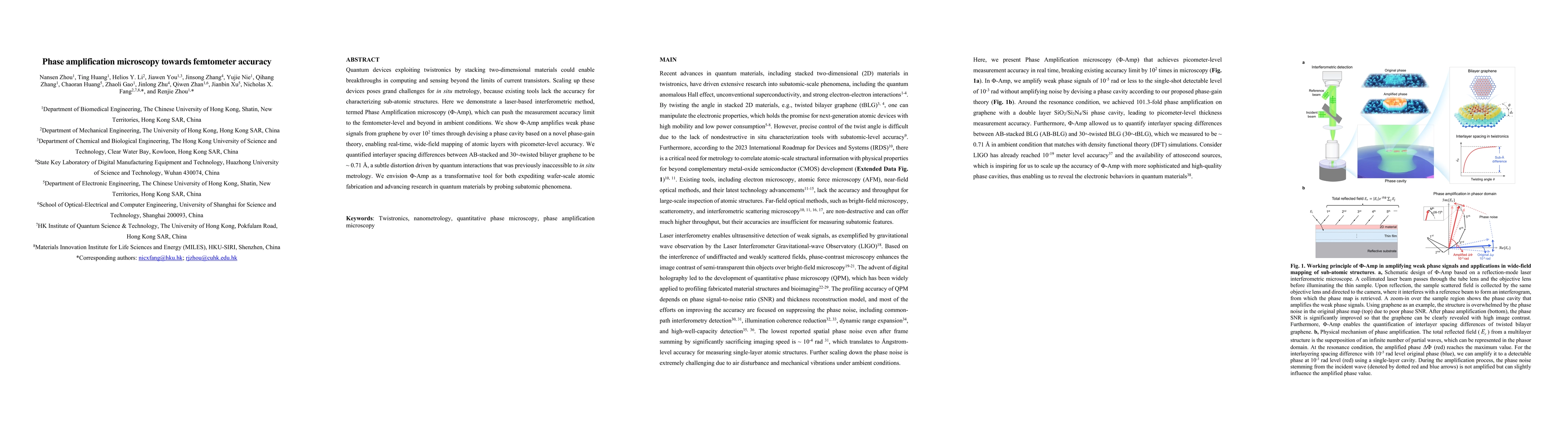
Quantum devices exploiting twistronics by stacking two-dimensional materials could enable breakthroughs in computing and sensing beyond the limits of current transistors. Scaling up these devices pose...

This website uses cookies to ensure you get the best experience. Learn more