Academic Profile
Statistics
Similar Authors
Papers on arXiv
Two-dimensional (2D) semiconducting transition-metal dichalcogenides (TMDCs) are an exciting platform for new excitonic physics and next-generation electronics, creating a strong demand to understan...
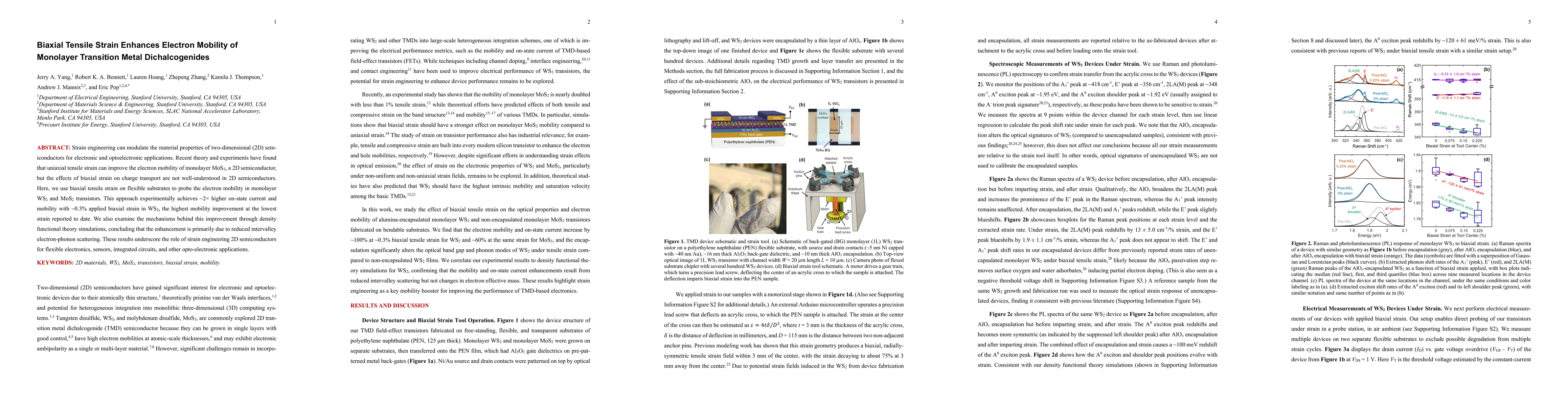
Strain engineering can modulate the material properties of two-dimensional (2D) semiconductors for electronic and optoelectronic applications. Recent theory and experiments have found that uniaxial ...
Bandgap control is of central importance for semiconductor technologies. The traditional means of control is to dope the lattice chemically, electrically or optically with charge carriers. Here, we ...
Strong coupling of two-dimensional semiconductor excitons with plasmonic resonators enables control of light-matter interaction at the subwavelength scale. Here we develop strong coupling in plasmon...
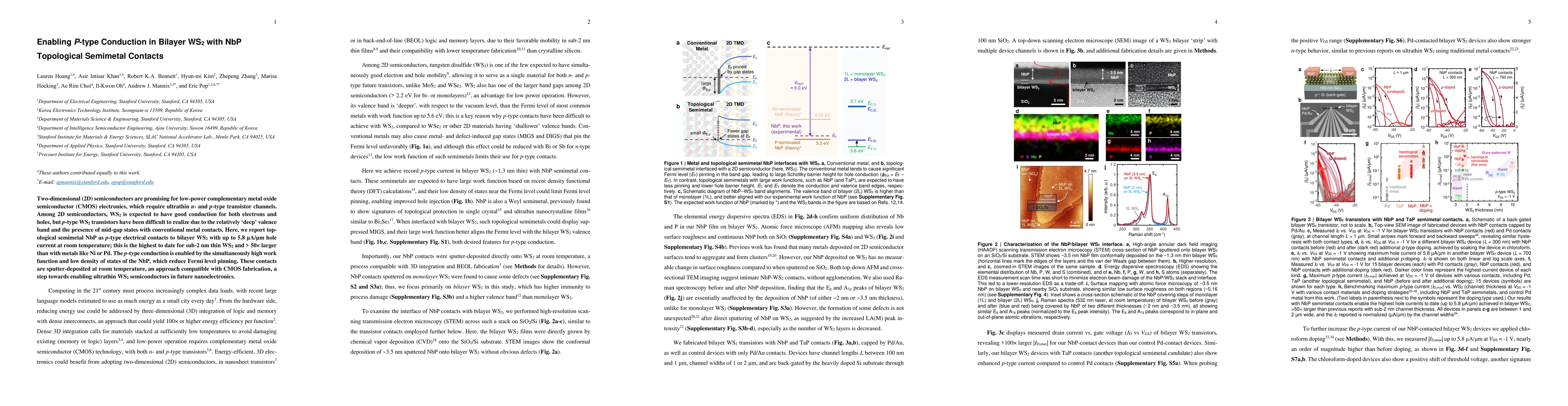
Two-dimensional (2D) semiconductors are promising for low-power complementary metal oxide semiconductor (CMOS) electronics, which require ultrathin n- and p-type transistor channels. Among 2D semicond...
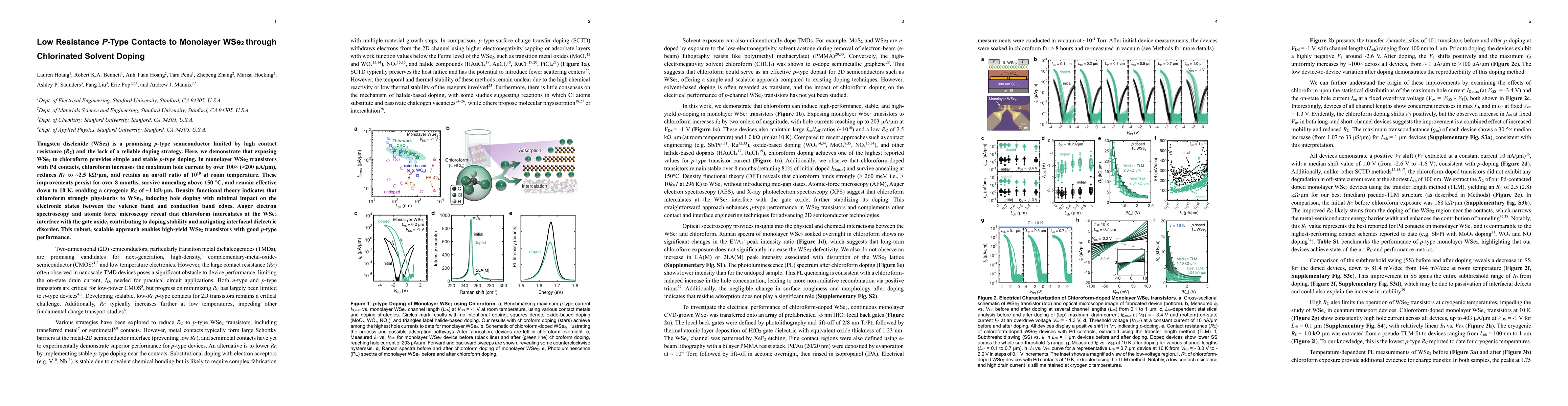
Tungsten diselenide (WSe$_2$) is a promising p-type semiconductor limited by high contact resistance ($R_\textrm{C}$) and the lack of a reliable doping strategy. Here, we demonstrate that exposing WSe...
Electronic and optoelectronic applications of two-dimensional (2D) semiconductors demand precise control over material quality, including thickness, composition, doping, and defect density. Convention...
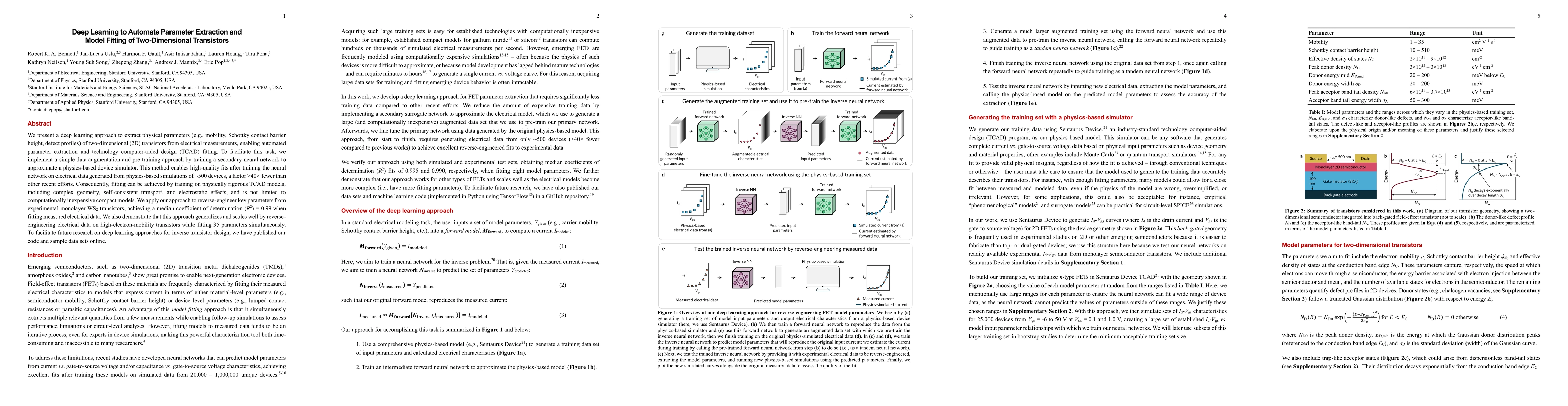
We present a deep learning approach to extract physical parameters (e.g., mobility, Schottky contact barrier height, defect profiles) of two-dimensional (2D) transistors from electrical measurements, ...
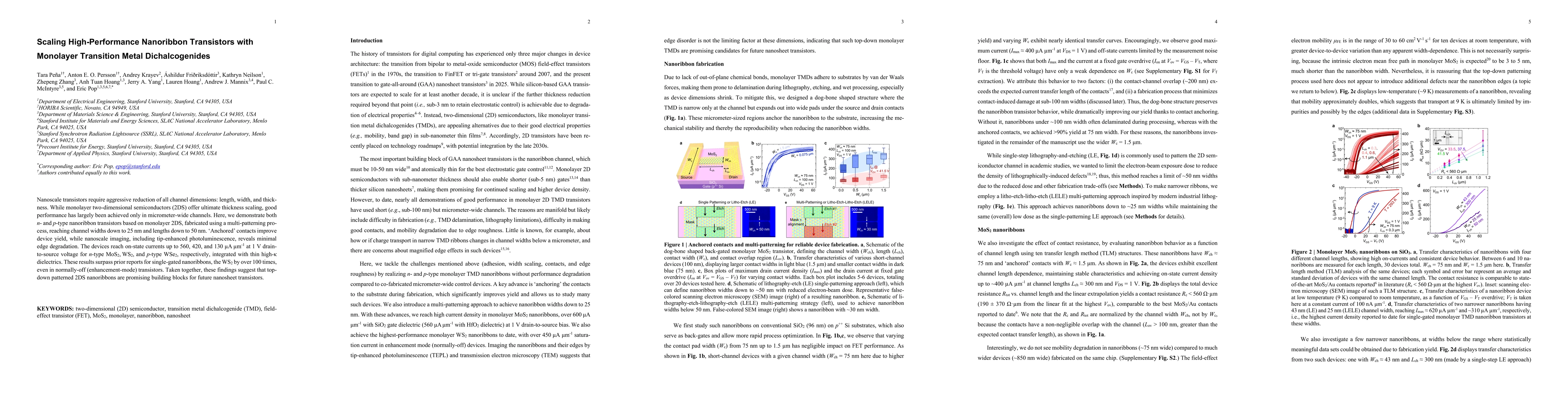
Nanoscale transistors require aggressive reduction of all channel dimensions: length, width, and thickness. While monolayer two-dimensional semiconductors (2DS) offer ultimate thickness scaling, good ...
Two-dimensional transition metal dichalcogenides (TMDCs) are promising materials for next-generation optoelectronic devices, yet their implementation is hindered by limited sample stability and challe...