ArxivLens
Z
Researcher

Zijin Lei

9 papers on arXiv

9 arXiv Papers
3 Total Publications
Profile

Academic Profile

Name Z. Lei
Total Papers 3
Scholar Profile View on Semantic Scholar
Metrics

Statistics

9 arXiv Papers
3 Total Publications
Publications

Papers on arXiv

Thumbnail for Gate-defined Two-dimensional Hole and Electron Systems in an Undoped
  InSb Quantum Well
arXiv
Gate-defined Two-dimensional Hole and Electron Systems in an Undoped InSb Quantum Well

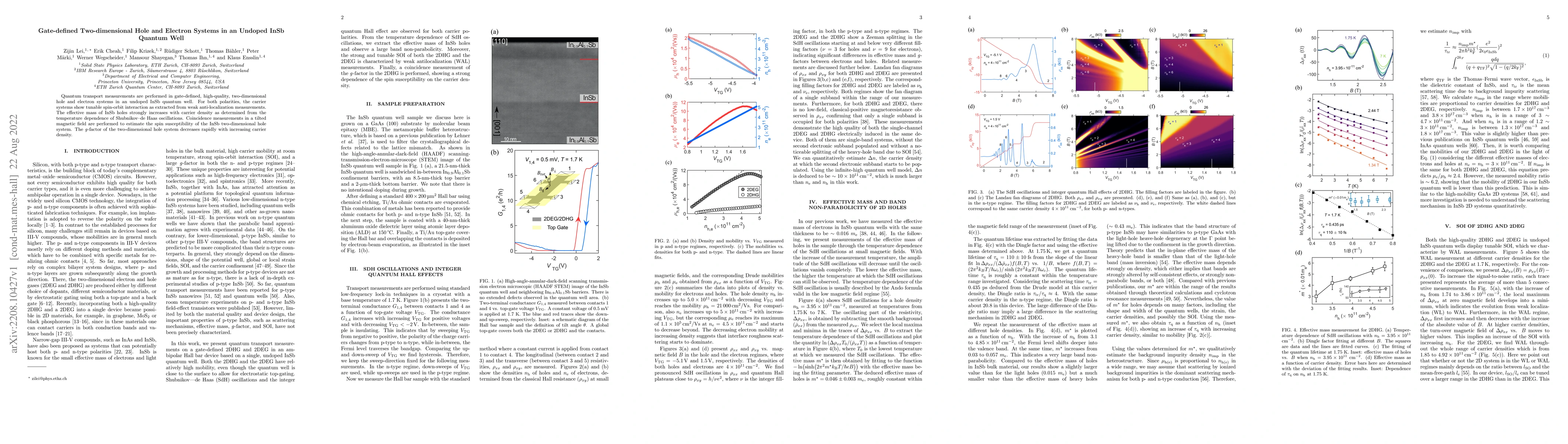
Quantum transport measurements are performed in gate-defined, high-quality, two-dimensional hole and electron systems in an undoped InSb quantum well. For both polarities, the carrier systems show t...

Thumbnail for High-quality Two-Dimensional Electron Gas in Undoped InSb Quantum Wells
arXiv
High-quality Two-Dimensional Electron Gas in Undoped InSb Quantum Wells

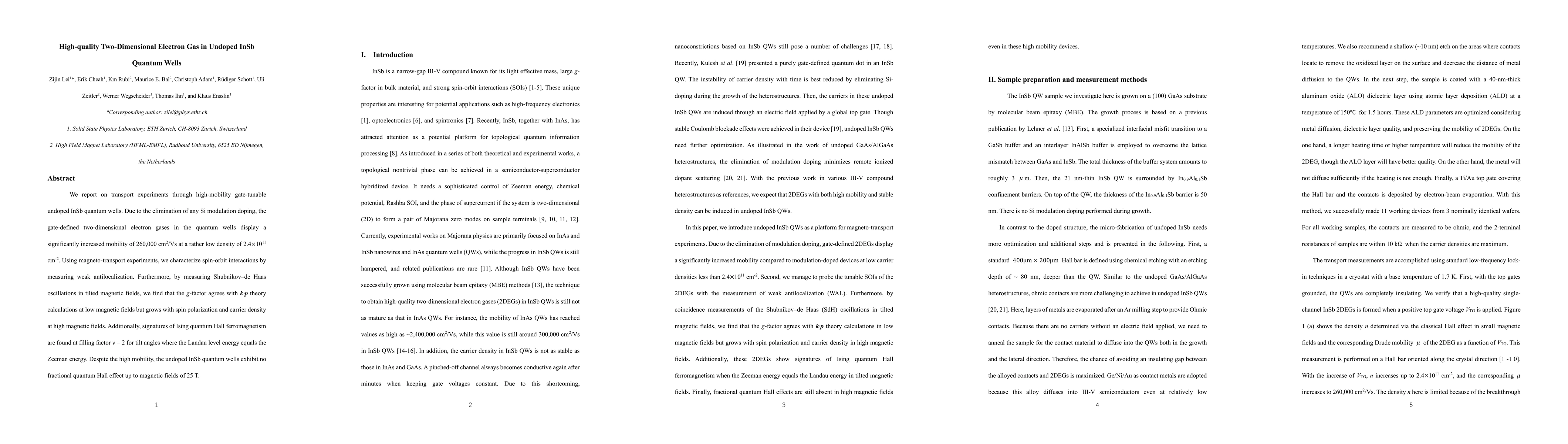
We report on transport experiments through high-mobility gate-tunable undoped InSb QWs. Due to the elimination of any Si modulation doping, the gate-defined two-dimensional electron gases in the qua...

Thumbnail for Electronic g-factor and Magneto-transport in InSb Quantum Wells
arXiv
Electronic g-factor and Magneto-transport in InSb Quantum Wells

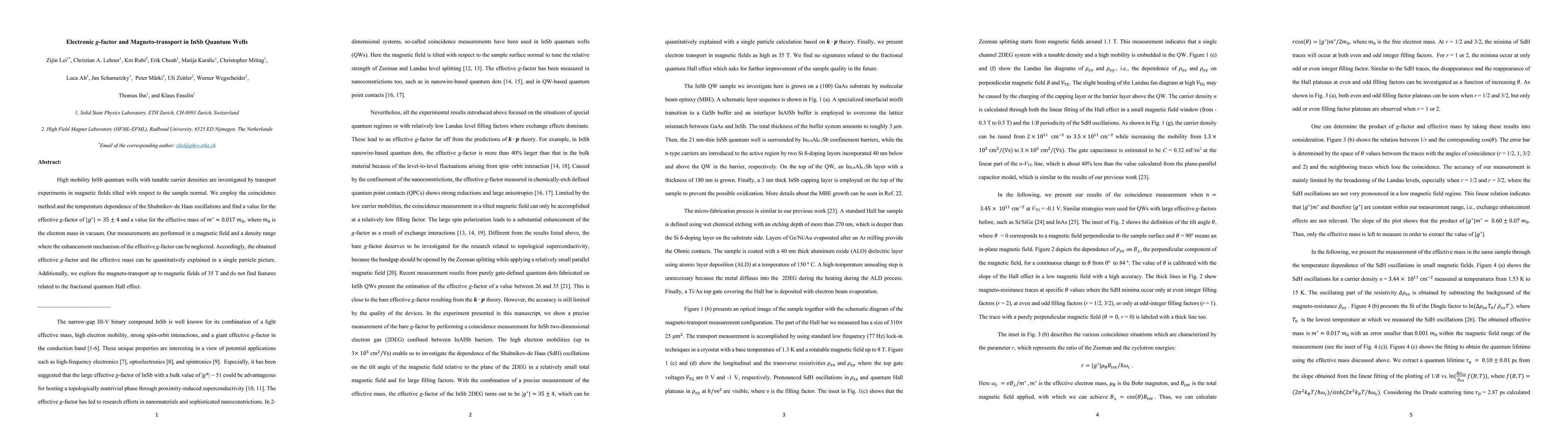
High mobility InSb quantum wells with tunable carrier densities are investigated by transport experiments in magnetic fields tilted with respect to the sample normal. We employ the coincidence metho...

Thumbnail for Quantum transport in high-quality shallow InSb quantum wells
arXiv
Quantum transport in high-quality shallow InSb quantum wells

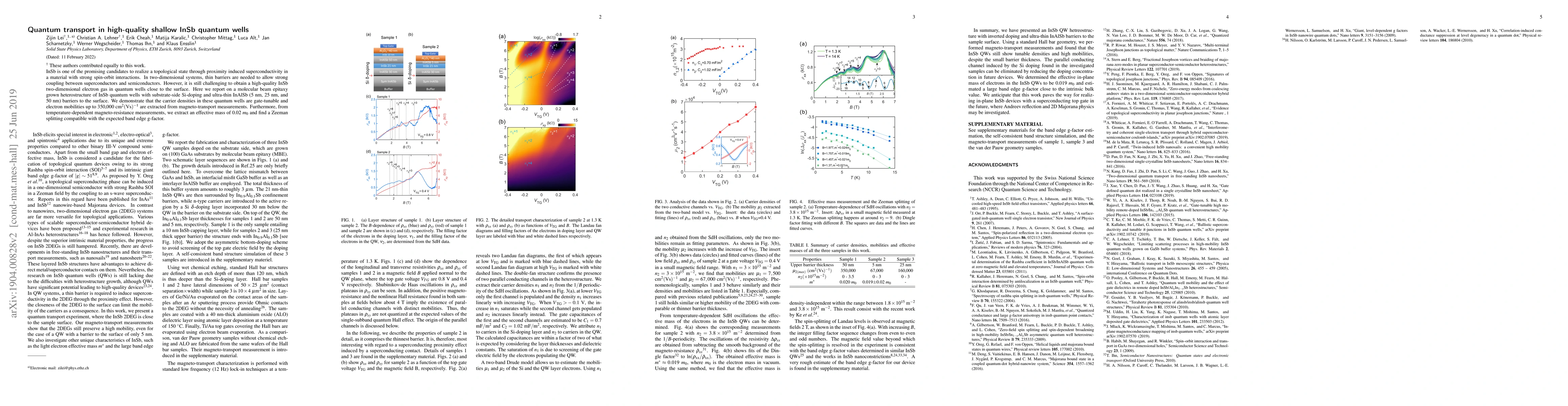
InSb is one of the promising candidates to realize a topological state through proximity induced superconductivity in a material with strong spin-orbit interactions. In two-dimensional systems, thin...

Thumbnail for Edgeless and Purely Gate-Defined Nanostructures in InAs Quantum Wells
arXiv
Edgeless and Purely Gate-Defined Nanostructures in InAs Quantum Wells

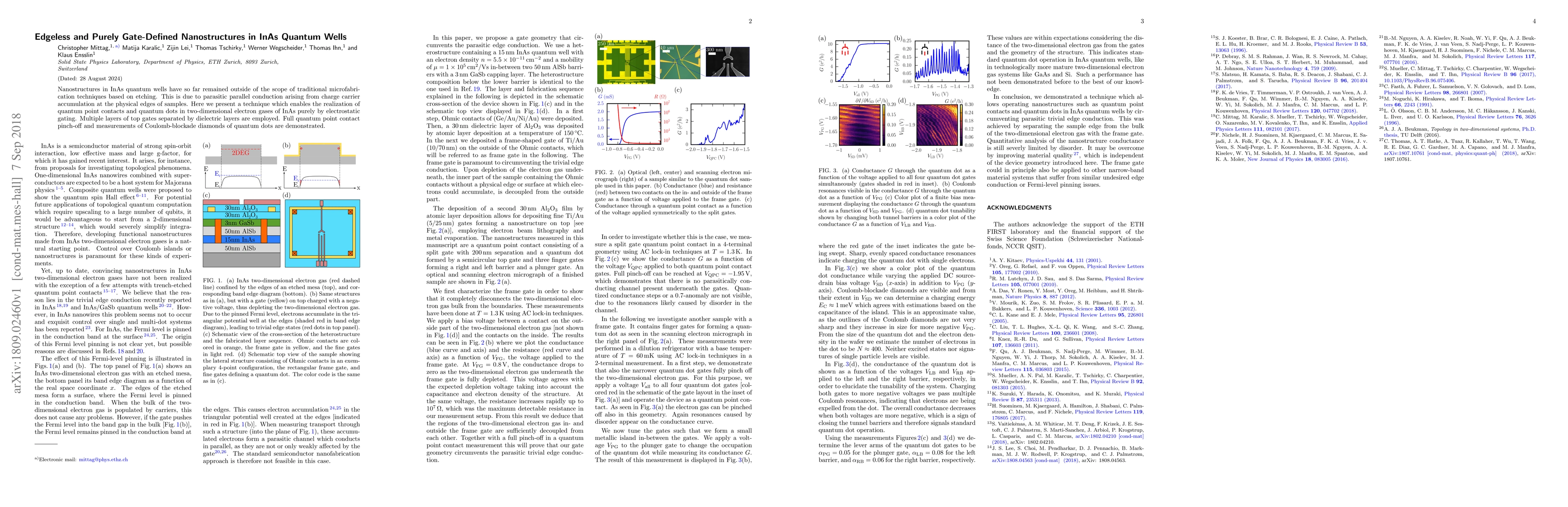
Nanostructures in InAs quantum wells have so far remained outside of the scope of traditional microfabrication techniques based on etching. This is due to parasitic parallel conduction arising from ...

Thumbnail for Memory resistor based in GaAs 2D-bilayers: In and out of equilibrium
arXiv
Memory resistor based in GaAs 2D-bilayers: In and out of equilibrium

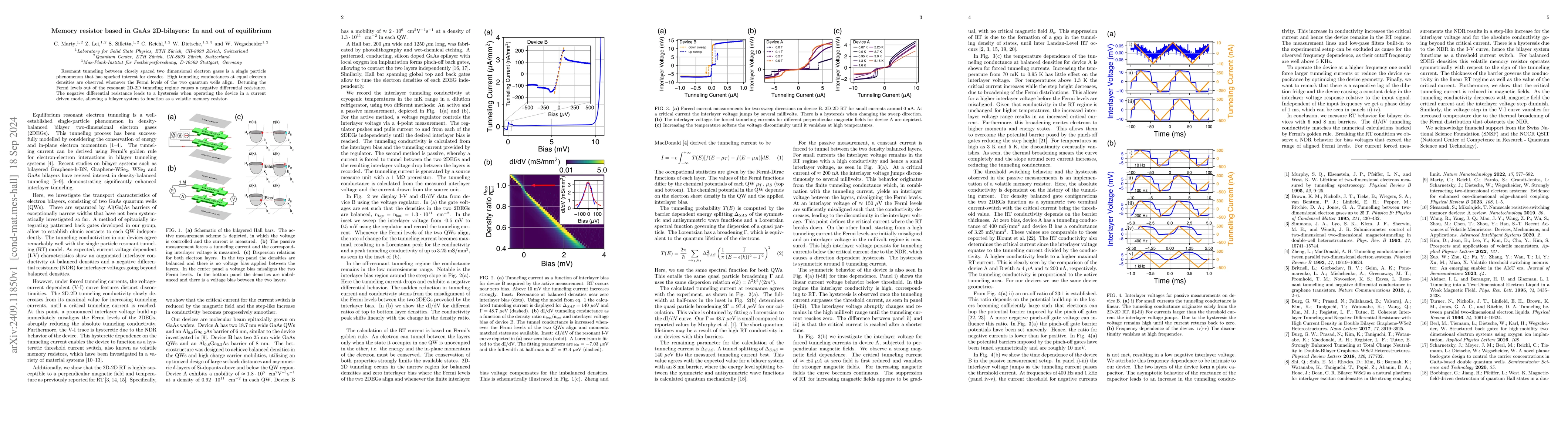
Resonant tunneling between closely spaced two dimensional electron gases is a single particle phenomenon that has sparked interest for decades. High tunneling conductances at equal electron densities ...

Thumbnail for Improving Electrical Contact Quality and Extraordinary Magnetoresistance
  in High Mobility III-V Semiconductors
arXiv
Improving Electrical Contact Quality and Extraordinary Magnetoresistance in High Mobility III-V Semiconductors

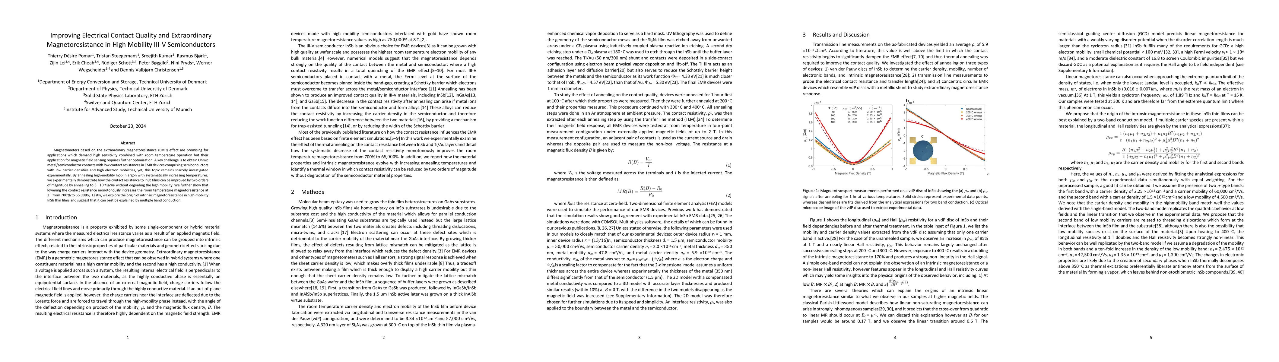
Magnetometers based on the extraordinary magnetoresistance (EMR) effect are promising for applications which demand high sensitivity combined with room temperature operation but their application for ...

Thumbnail for An InAsSb surface quantum well with in-situ deposited Nb as a platform
  for semiconductor-superconductor hybrid devices
arXiv
An InAsSb surface quantum well with in-situ deposited Nb as a platform for semiconductor-superconductor hybrid devices

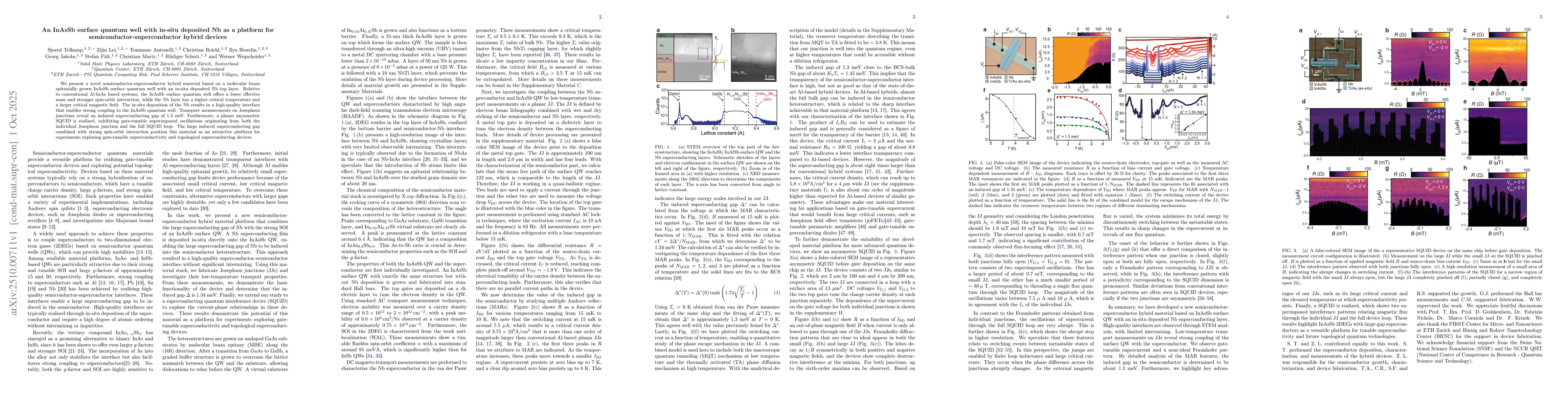
We present a novel semiconductor-superconductor hybrid material based on a molecular beam epitaxially grown InAsSb surface quantum well with an in-situ deposited Nb top layer. Relative to conventional...

Thumbnail for Impact of Layer Structure and Strain on Morphology and Electronic Properties of InAs Quantum Wells on InP (001)
arXiv
Impact of Layer Structure and Strain on Morphology and Electronic Properties of InAs Quantum Wells on InP (001)

High-quality InAs quantum wells grown on InP are a promising platform for topological quantum information processing due to their large g-factor, strong Rashba spin-orbit interaction, and their compat...

This website uses cookies to ensure you get the best experience. Learn more