Publication
Metrics
Paper Preview
Abstract
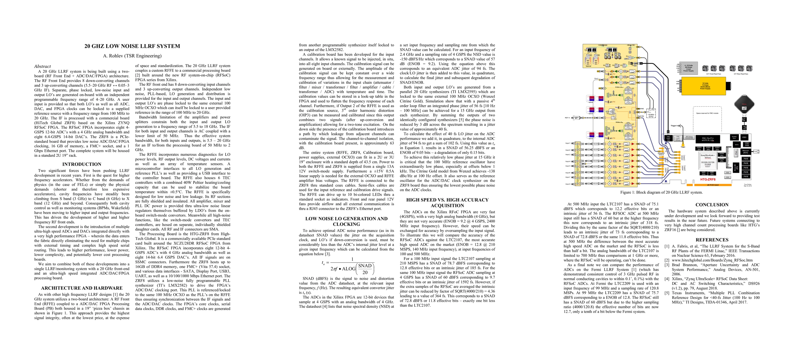
A 20 GHz LLRF system is being built using a two-board(RF Front End + ADC/DAC/FPGA) architecture. The RF Front End provides 8 down-converting channels and 3 up-converting channels (5.5-20 GHz RF to 0.05-3 GHz IF). Separate, phase locked, low-noise input and output LO's are generated on-board with an independent programmable frequency range of 4-20 GHz. A user input is provided so that both LO's as well as all ADC, DAC, and FPGA clocks can be locked to a supplied reference source with a frequency range from 100 MHz to 20 GHz. The IF is processed with a commercial board (HiTech Global ZRF8) based on the Xilinx ZYNQ RFSoC FPGA. The RFSoC FPGA incorporates eight 4-GSPS 12-bit ADC's with a 4 GHz analog bandwidth and eight 6.4-GSPS 14-bit DAC's. The ZRF8 is a PCIe-standard board that provides low noise ADC/DAC/FPGA clocking, 16 GB of memory, a FMC+ socket, and a 1 Gbps Ethernet port. The complete system will be housed in a standard 2U 19" rack.
AI Key Findings
Get AI-generated insights about this paper's methodology, results, significance, and more — seven facets brought into focus.
Impact
Paper Details
Authors
PDF Preview
Key Terms
Citation Network
Current paper (gray), citations (green), references (blue)
Display is limited for performance on very large graphs.
Discussion 0