2D Addressable Mid-infrared Metasurface Spatial Light Modulator
Publication
Metrics
Paper Preview
Abstract
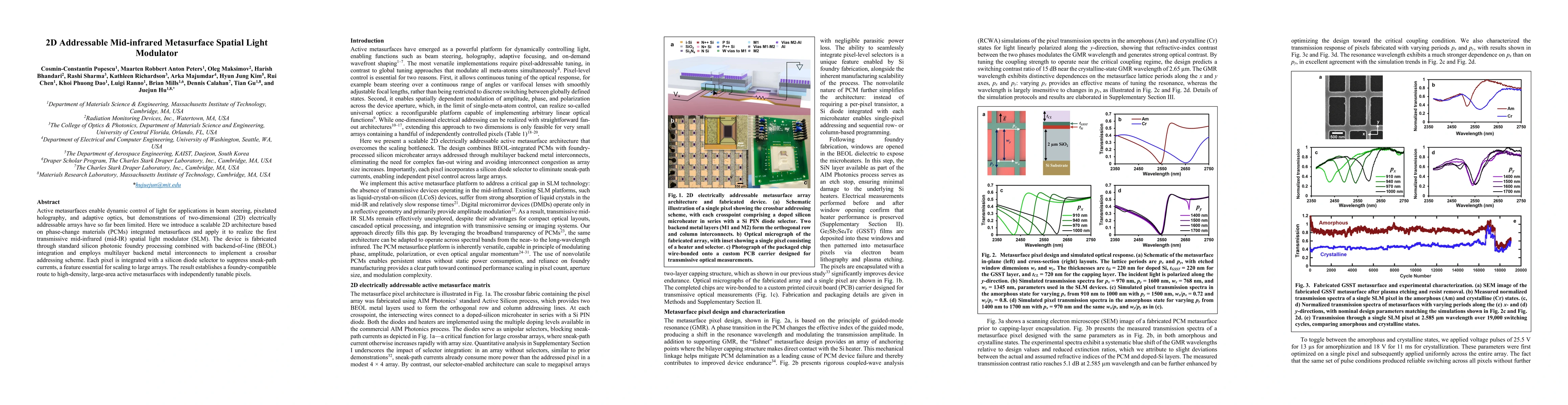
Active metasurfaces enable dynamic control of light for applications in beam steering, pixelated holography, and adaptive optics, but demonstrations of two-dimensional (2D) electrically addressable arrays have so far been limited. Here we introduce a scalable 2D architecture based on phase-change materials (PCMs) integrated metasurfaces and apply it to realize the first transmissive mid-infrared (mid-IR) spatial light modulator (SLM). The device is fabricated through standard silicon photonic foundry processing combined with backend-of-line (BEOL) integration and employs multilayer backend metal interconnects to implement a crossbar addressing scheme. Each pixel is integrated with a silicon diode selector to suppress sneak-path currents, a feature essential for scaling to large arrays. The result establishes a foundry-compatible route to high-density, large-area active metasurfaces with independently tunable pixels.
AI Key Findings
Get AI-generated insights about this paper's methodology, results, significance, and more — seven facets brought into focus.
Discussion 0