Summary

2D materials are compatible with many material platforms as they adhere to other materials strictly by van der Waals interactions. This, together with the variety of band gaps found among transition metal dichalcogenides (TMDCs), makes them uniquely interesting to study for on-chip light sources, as the photonic integrated circuit (PIC) industry is developing into several material platforms depending on the application (gold, silicon, silicon nitride, indium phosphide, etc). 2D materials could thus potentially provide a universal on-chip light source (and detector) scheme for all PIC platforms in the future. Here we show recent results on how exfoliated monolayer TMDC flakes can be integrated with plasmonic slot-waveguides and plasmonic dipole antenna couplers to inject their photoluminescence into plasmonic waveguides as a first step towards future on-chip light sources for such systems.

AI Key Findings

Generated Sep 02, 2025

Methodology

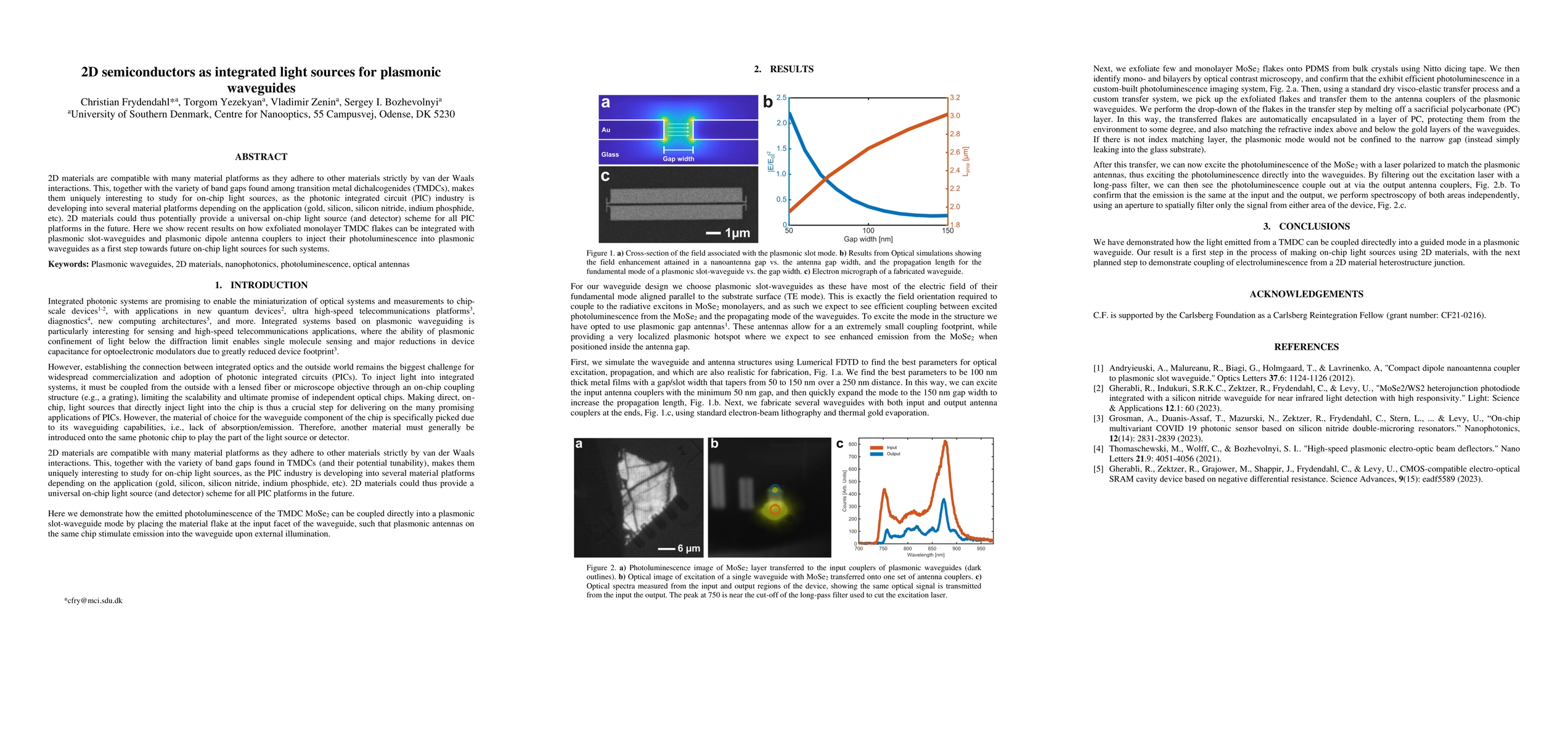
The research demonstrates the integration of exfoliated monolayer TMDC flakes, specifically MoSe2, with plasmonic slot-waveguides and plasmonic dipole antenna couplers. Optical simulations and electron microscopy are employed to optimize the waveguide and antenna structures, followed by fabrication using electron-beam lithography and thermal gold evaporation.

Key Results

  • Successful coupling of photoluminescence from MoSe2 into plasmonic slot-waveguide modes.
  • Efficient excitation of the plasmonic antenna couplers leading to enhanced emission from MoSe2 within the antenna gap.
  • Demonstration of light transmission from input to output antenna couplers, confirming the integrity of the optical signal.

Significance

This work is significant as it represents a first step towards on-chip light sources using 2D materials, which could potentially provide a universal light source and detector scheme for various PIC platforms, addressing the challenge of integrating light sources directly onto photonic chips.

Technical Contribution

The study presents a novel method for directly coupling the photoluminescence of 2D materials into plasmonic waveguides using plasmonic antennas, paving the way for on-chip light sources in photonic integrated circuits.

Novelty

This research is novel due to its focus on utilizing 2D materials, particularly TMDCs, for on-chip light sources, offering a potential universal solution for various PIC platforms, which has not been extensively explored in prior studies.

Limitations

  • The current study only demonstrates coupling of photoluminescence from MoSe2; future work should focus on coupling electroluminescence from 2D material heterostructure junctions.
  • The research is limited to MoSe2 and plasmonic slot-waveguides; further investigation is needed to validate compatibility with other 2D materials and waveguide types.

Future Work

  • Demonstrate coupling of electroluminescence from 2D material heterostructure junctions.
  • Explore compatibility with a broader range of 2D materials and waveguide designs.

Paper Details

PDF Preview

Download PDF

Citation Network

Current paper (gray), citations (green), references (blue)

Display is limited for performance on very large graphs.

Current Paper
Citations
References
Click to view

No citations found for this paper.

Comments (0)

This website uses cookies to ensure you get the best experience. Learn more