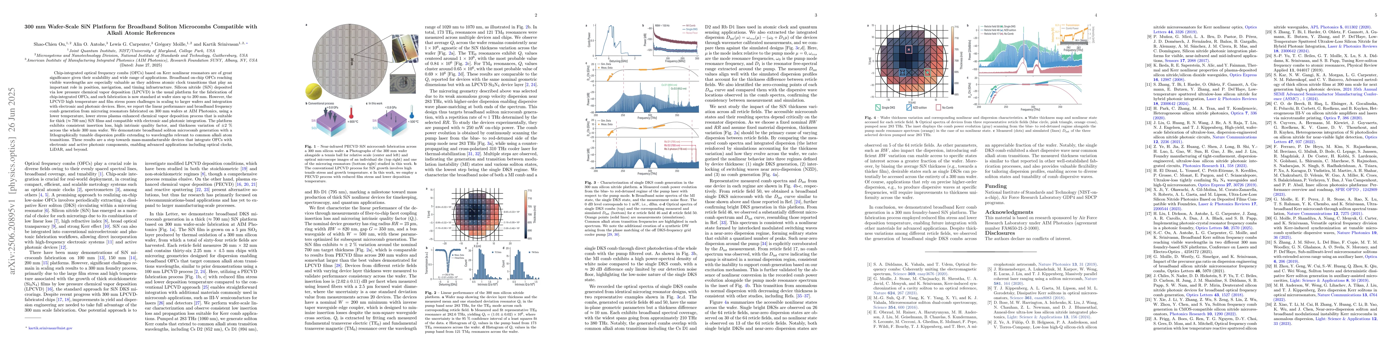
Chip-integrated optical frequency combs (OFCs) based on Kerr nonlinear
resonators are of great significance given their scalability and wide range of
applications. Broadband on-chip OFCs reaching visible wavelengths are
especially valuable as they address atomic clock transitions that play an
important role in position, navigation, and timing infrastructure. Silicon
nitride (SiN) deposited via low pressure chemical vapor deposition (LPCVD) is
the usual platform for the fabrication of chip-integrated OFCs, and such
fabrication is now standard at wafer sizes up to 200 mm. However, the LPCVD
high temperature and film stress poses challenges in scaling to larger wafers
and integration with electronic and photonic devices. Here, we report the
linear performance and broadband frequency comb generation from microring
resonators fabricated on 300 mm wafers at AIM Photonics, using a lower
temperature, lower stress plasma enhanced chemical vapor deposition process
that is suitable for thick ($\approx$ 700 nm) SiN films and compatible with
electronic and photonic integration. The platform exhibits consistent insertion
loss, high intrinsic quality factor, and thickness variation of $\pm$2 % across
the whole 300 mm wafer. We demonstrate broadband soliton microcomb generation
with a lithographically tunable dispersion profile extending to wavelengths
relevant to common alkali atom transitions. These results are a step towards
mass-manufacturable devices that integrate OFCs with electronic and active
photonic components, enabling advanced applications including optical clocks,
LiDAR, and beyond.
Discussion 0