3D interconnects have emerged as a solution to address the scaling issues of
interconnect bandwidth and the memory wall problem in high-performance
computing (HPC), such as High-Bandwidth Memory (HBM). However, the copper-based
electrical interconnect retains fundamental limitations. Dense I/O for
high-speed signals lead to degraded signal quality for end-to-end links,
necessitating additional circuits to mitigate signal impairments and resulting
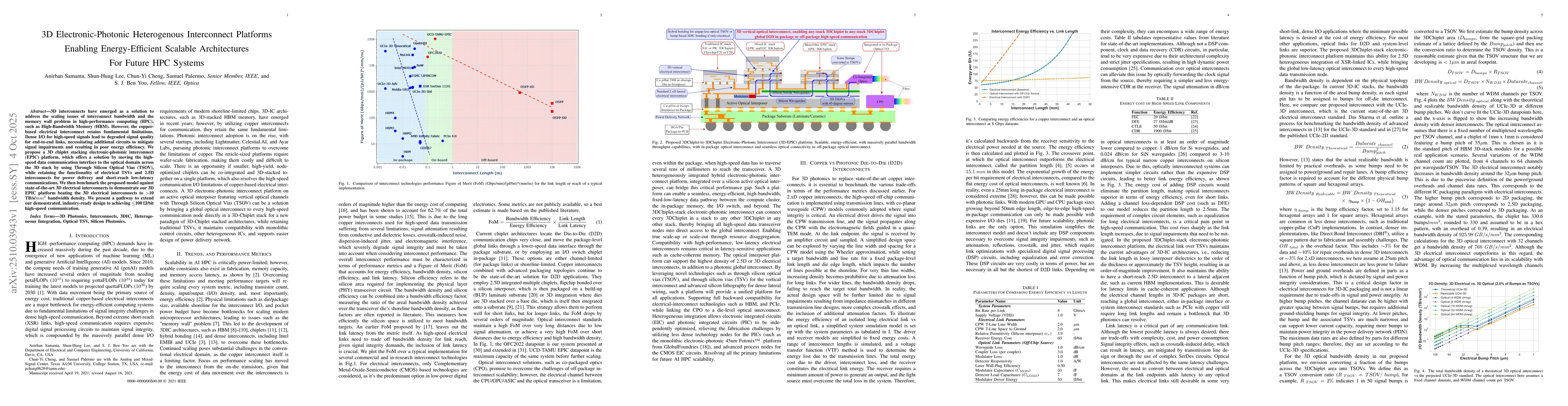
in poor energy efficiency. We propose a 3D chiplet stacking electronic-photonic
interconnect (EPIC) platform, which offers a solution by moving the high-speed
data communication interface to the optical domain across the 3D stack by using
Through Silicon Optical Vias (TSOV), while retaining the functionality of
electrical TSVs and 2.5D interconnects for power delivery and short-reach
low-latency communications. We then benchmark the proposed model against
state-of-the-art 3D electrical interconnects to demonstrate our 3D EPIC
platform beating the 3D electrical interconnects to $>$10 TB/s/$mm^2$ bandwidth
density. We present a pathway to extend our demonstrated, industry-ready design
to achieving $\leq$100 fJ/bit high-speed communication.
Discussion 0