Summary
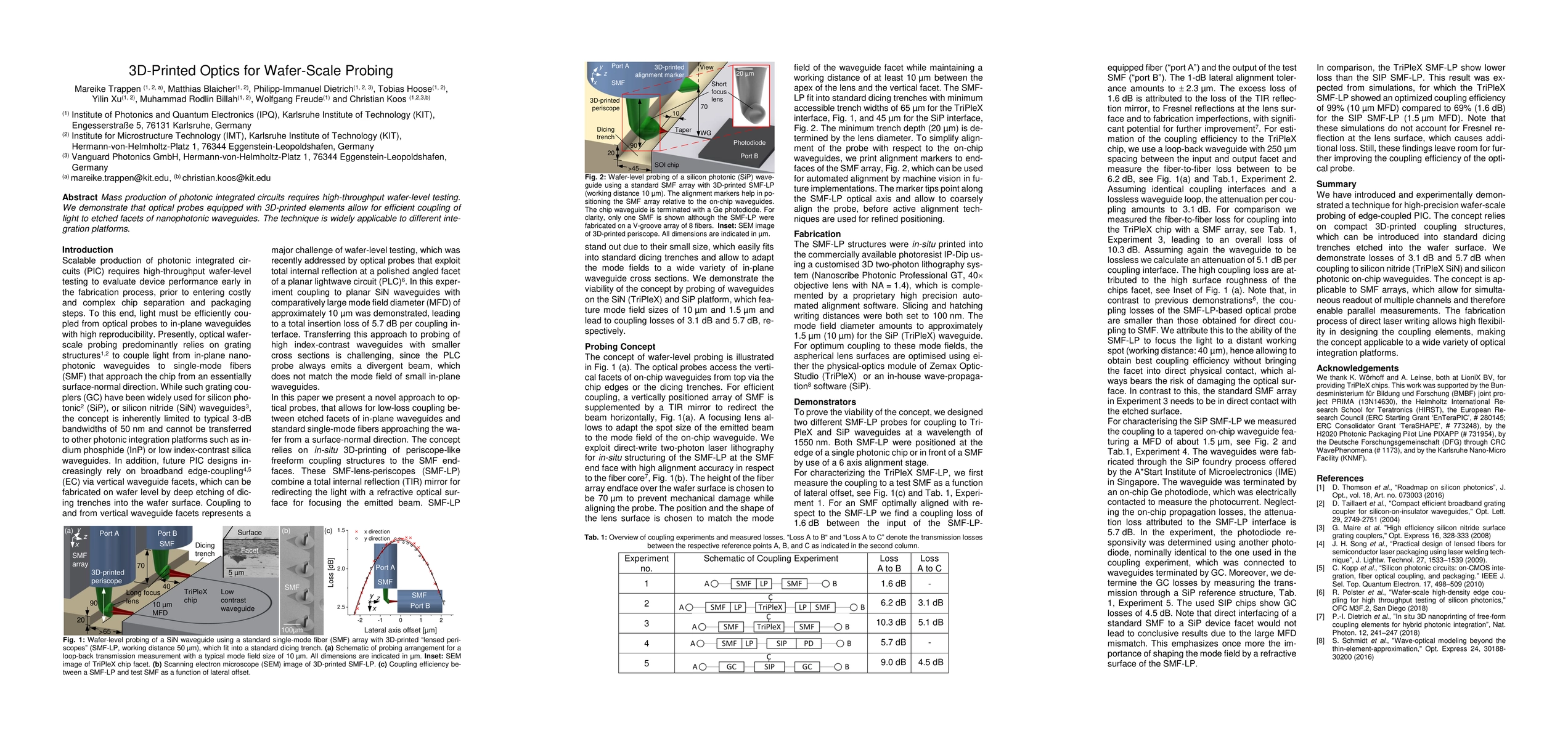
Mass production of photonic integrated circuits requires high-throughput wafer-level testing. We demonstrate that optical probes equipped with 3D-printed elements allow for efficient coupling of light to etched facets of nanophotonic waveguides. The technique is widely applicable to different integration platforms.
AI Key Findings
Get AI-generated insights about this paper's methodology, results, and significance.
Paper Details
PDF Preview
Key Terms
Citation Network
Current paper (gray), citations (green), references (blue)
Display is limited for performance on very large graphs.
Similar Papers
Found 4 papersTransformation-optics modeling of 3D-printed freeform waveguides
Tudor Olariu, Carsten Rockstuhl, Willy Dörfler et al.
Miniature 120-beam coherent combiner with 3D printed optics for multicore fiber based endoscopy
Esben Ravn Andresen, Siddharth Sivankutty, Hervé Rigneault et al.
Wafer-Scale Fast Fourier Transforms
Ilya Sharapov, Robert Schreiber, Marcelo Orenes-Vera et al.
| Title | Authors | Year | Actions |
|---|

Comments (0)